-
BackX
-
Components
-
-
Category
-
Semiconductors
- Diodes
- Thyristors
-
Electro-insulated Modules
- Electro-insulated Modules | VISHAY (IR)
- Electro-insulated Modules | INFINEON (EUPEC)
- Electro-insulated Modules | Semikron
- Electro-insulated Modules | POWEREX
- Electro-insulated Modules | IXYS
- Electro-insulated Modules | POSEICO
- Electro-insulated Modules | ABB
- Electro-insulated Modules | TECHSEM
- Go to the subcategory
- Bridge Rectifiers
-
Transistors
- Transistors | GeneSiC
- SiC MOSFET Modules | Mitsubishi
- SiC MOSFET Modules | STARPOWER
- Module SiC MOSFET ABB’s
- IGBT Modules | MITSUBISHI
- Transistor Modules | MITSUBISHI
- MOSFET Modules | MITSUBISHI
- Transistor Modules | ABB
- IGBT Modules | POWEREX
- IGBT Modules | INFINEON (EUPEC)
- Silicon Carbide (SiC) semiconductor elements
- Go to the subcategory
- Gate Drivers
- Power Blocks
- Go to the subcategory
- Electrical Transducers
-
Passive components (capacitors, resistors, fuses, filters)
- Resistors
-
Fuses
- Miniature Fuses for electronic circuits - ABC & AGC Series
- Tubular Fast-acting Fuses
- Time-delay Fuse Links with GL/GG & AM characteristics
- Ultrafast Fuse Links
- Fast-acting Fuses (British & American standard)
- Fast-acting Fuses (European standard)
- Traction Fuses
- High-voltage Fuse Links
- Go to the subcategory
- Capacitors
- EMI Filters
- Supercapacitors
- Power surge protection
- Go to the subcategory
-
Relays and Contactors
- Relays and Contactors - Theory
- 3-Phase AC Semiconductor Relays
- DC Semiconductor Relays
- Controllers, Control Systems and Accessories
- Soft Starters and Reversible Relays
- Electromechanical Relays
- Contactors
- Rotary Switches
-
Single-Phase AC Semiconductor Relays
- AC ONE PHASE RELAYS 1 series| D2425 | D2450
- One phase semiconductor AC relays CWA and CWD series
- One phase semiconductor AC relays CMRA and CMRD series
- One phase semiconductor AC relays - PS series
- Double and quadruple semiconductor AC relays - D24 D, TD24 Q, H12D48 D series
- One phase semiconductor relays - gn series
- Ckr series single phase solid state relays
- One phase AC semiconductor relays for DIN bus - ERDA I ERAA series
- 150A AC single phase relays
- Rail Mountable Solid State Relays With Integrated Heat Sink - ENDA, ERDA1 / ERAA1 series
- Go to the subcategory
- Single-Phase AC Semiconductor Relays for PCBs
- Interface Relays
- Go to the subcategory
- Cores and Other Inductive Components
- Heatsinks, Varistors, Thermal Protection
- Fans
- Air Conditioning, Accessories for Electrical Cabinets, Coolers
-
Batteries, Chargers, Buffer Power Supplies and Inverters
- Batteries, Chargers - Theoretical Description
- Modular Li-ion Battery Building Blocks, Custom Batteries, BMS
- Batteries
- Battery Chargers and Accessories
- Uninterruptible Power Supply and Buffer Power Supplies
- Inverters and Photovoltaic Equipments
- Energy storage
- Fuel cells
- Lithium-ion batteries
- Go to the subcategory
-
Automatics
- Futaba Drone Parts
- Limit Switches, Microswitches
- Sensors, Transducers
-
Infrared Thermometers (Pyrometers)
- IR-TE Series - Water-proof Palm-sized Radiation Thermometer
- IR-TA Series - Handheld Type Radiation Thermometer
- IR-H Series - Handheld Type Radiation Thermometer
- IR-BA Series - High-speed Compact Radiation Thermometer
- IR-FA Series - Fiber Optic Radiation Thermometer
- IR-BZ Series - Compact Infrared Thermometers
- Go to the subcategory
- Counters, Time Relays, Panel Meters
- Industrial Protection Devices
- Light and Sound Signalling
- Thermographic Camera
- LED Displays
- Control Equipments
-
Recorders
- Hybrid Recorders - AL3000 Series | CHINO
- Graphic Recorder - KR2000 Series | CHINO
- Ubiquitous Recorders - KR5000 Series | CHINO
- Palm-sized Temperature/Humidity Meters - HN-CH Series | CHINO
- Consumables for Recorders
- 71VR1 - Compact Paperless Recorder | M-SYSTEM
- Graphic Recorder - KR3000 Series | CHINO
- PC Recorders - R1M Series | M-SYSTEM
- PC Recorders - R2M Series | M-SYSTEM
- PC Recorders - RZMS Series | M-SYSTEM
- PC Recorders - RZUS Series | M-SYSTEM
- Go to the subcategory
- Go to the subcategory
-
Cables, Litz wires, Conduits, Flexible connections
- Wires
- Litz wires
- Cables for extreme applications
- Sleevings
-
Braids
- Flat Braids
- Round Braids
- Very Flexible Flat Braids
- Very Flexible Round Braids
- Cylindrical Cooper Braids
- Cylindrical Cooper Braids and Sleevings
- Flexible Earthing Connections
- Galvanized and Stainless Steel Cylindrical Braids
- PCV Insulated Copper Braids (temp. up to 85C)
- Flat Aluminium Braids
- Junction Set - Braids and Tubes
- Go to the subcategory
- Traction Equipment
- Cable Terminals
- Flexible Insulated Busbars
- Flexible Multilayer Busbars
- Cable Duct Systems
- Hoses
- Go to the subcategory
- View all categories
-
Semiconductors
-
-
- Suppliers
-
Applications
- CNC Machine Tools
- DC and AC Drives (Inverters)
- Energetics
- Energy bank
- Equipment and Components for Hazardous Areas [Ex]
- Equipment for Distribution, Control and Telecommunications Cabinets
- HVAC Automation
- Induction Heating
- Industrial Automation
- Industrial Protective Devices
- Machines for Drying and Wood Processing
- Machines for Thermoforming Plastics
- Mining, Metallurgy and Foundry
- Motors and Transformers
- Power Supplies (UPS) and Rectifier Systems
- Printing
- Temperature Measurement and Regulation
- Test and Laboratory Measurements
- Tram and Railway Traction
- Welding Machines
-
Assembly
-
-
Inductors
-
-
Induction devices
-
-
https://www.dacpol.eu/pl/naprawy-i-modernizacje
-
-
Service
-
- Contact
- Zobacz wszystkie kategorie
New 800A/1200V Full SiC Module

New 800A/1200V Full SiC Module
By using SiC-based semiconductors the performance of power electronic systems can be drastically improved.
By Eckhard Thal, Koichi Masuda and Eugen Wiesner, Mitsubishi Electric Europe B.V., Ratingen, Germany
The evolution of SiC technology in power modules and its principle loss reduction potential are shown in Figure 1. Mitsubishi has developed two new full SiC module types with 800A and 1200A rated currents and 1200V rated voltage [1]; [2]. This article is describing the 800A module.
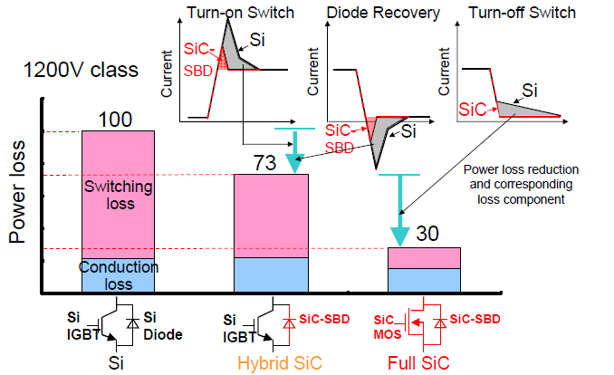
Figure 1: Evolution of SiC technology in power modules
Package outline and circuit diagram
The appearance of new 800A/1200V full SiC module (type name: FMF800DX-24A) and its internal circuit diagram are shown in Figure 2. The module contains 2 x 400A half bridge configurations. By externally paralleling the main P-, N- and AC-terminals an 800A/1200V 2in1 configuration is formed. By this paralleling approach the internal package inductance LS has been decreased to less than 10nH, which is important for limiting the overvoltage spikes at chip level due to high di/dt at switching of SiC-MOSFET.
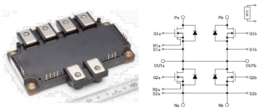
Figure 2: FMF800DX-24A package outline and internal circuit
The baseplate dimension of FMF800DX-24A is 62mm x 121mm. Thus the module size of new 800A/1200V full SiC module is about 1/2 compared with conventional Si-based IGBT modules having the same current rating, see Figure 3.

Figure 3: Footprint comparison
For monitoring the baseplate temperature TC a NTC-sensor located close to the MOSFET/FWDi chips is incorporated into the module. For short circuit and overcurrent protection MOSFET-chips with on-chip current sensing are used in one of the half bridge configurations (see Figure 2).
Main module parameters
The main parameters of 800A full SiC module are shown in Table 1.
The values of VDS, RDS(on) and VSD are given on chip level.
| Symbol | Parameter | FMF800DX-24A |
|---|---|---|
| VDSX | Drain-source voltage (at VGS=-15V) | 1200V (max) |
| ID | Drain current | 800A |
| ID(max) | Max. drain current (pulse) | 1600A |
| TJ(max) | Max. junction temperature | 150°C |
| VDS(on) | Drain-source On-voltage @ ID; TJ=150°C | 2,4V (typ) |
| RDS(on) | Drain-source On-resistance @ ID; TJ=150°C | 3,0mΩ (typ) |
| VSD | Source-drain voltage @ -ID; TJ=150°C | 2,2V (typ) |
| VGS(+) | Gate-source On-voltage | 13,5V…16,5V |
| VGS(-) | Gate-source Off-voltage | -9V…-16,5V |
| Rth(j-c)Q | MOSFET thermal resistance | 42 K/kW |
| Rth(j-c)D | FWDi thermal resistance | 61 K/kW |
Table 1: Main FMF800DX-24A parameters
Switching characteristics
Typical turn-on and turn-off switching waveforms at VCC=800V; TJ=150°C; RG(on)=RG(off)=5Ω are shown in Figure 4 and 5 for different drain currents ID=140A…1400A.
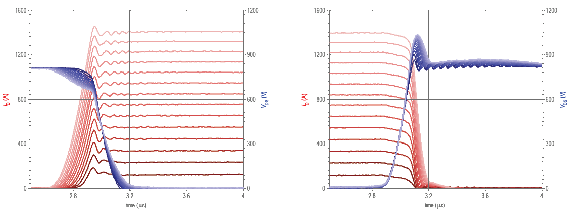
Figure 4: Turn-on waveforms / Figure 5: Turn-off waveforms
For limiting the turn-off overvoltage spike a cross-snubber capacitor of CS=6μF was connected between P- an N-terminals. The dependency of switching speed di/dt on drain current ID is shown in Figure 6 and 7 for different junction temperatures TJ=25°C; 75°C; 125°C; 150°C and different DC-link voltages VCC=600V; 800V.
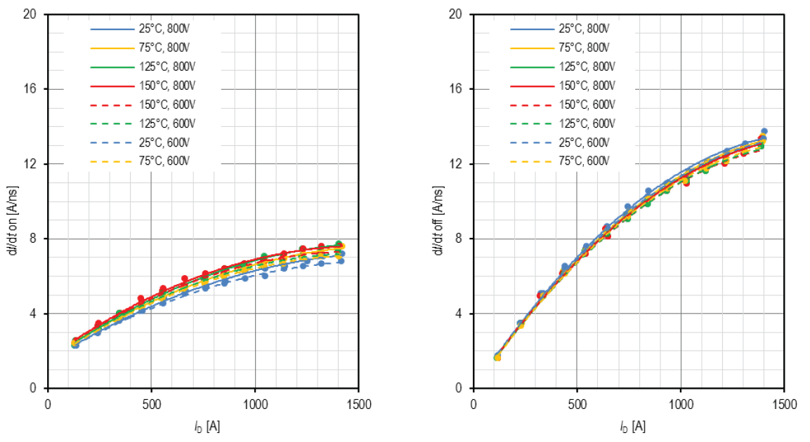
Figure 6: Turn-on di/dt versus ID / Figure 7: Turn-off di/dt versus ID
Two comments can be derived from Figure 6 and 7:
- The current slopes at turn–on and turn-off don’t show a strong dependency on chip temperature TJ and DC-link voltage VCC. This behavior differs from today’s IGBT-modules.
- The maximum di/dt at turning-off ID=1400A was about 13A/ns, which is quite similar to the switching speed known from today’s high current 1200V IGBT-modules.
Loss comparison with Si-based IGBT modules
The typical forward characteristics of new 800A full SiC module and existing 800A Si-based IGBT module are compared in Figure 8.
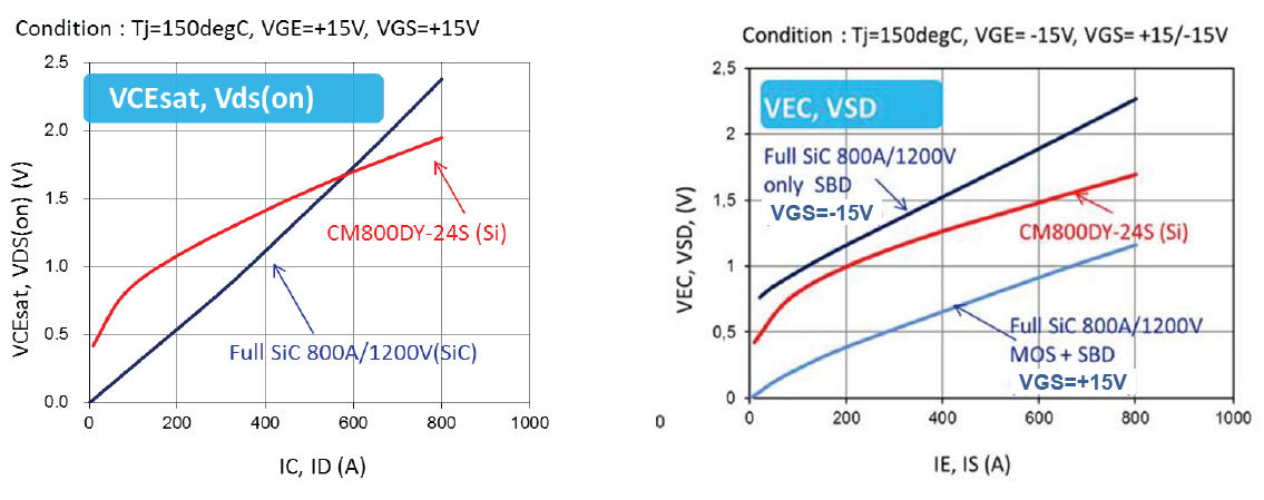
Figure 8: Forward characteristics
The comparison of switching energies in Figure 9 is indicating a key benefit of SiC technology: the switching losses can be drastically reduced compared with Si-based IGBT modules.
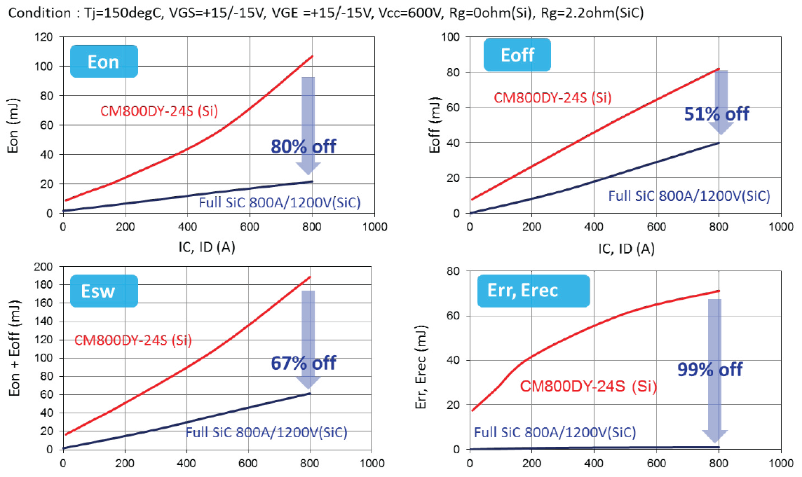
Figure 9: Switching energy comparison
This benefit can be seen in the power loss simulation results per Transistor/ FWDi-pair in inverter operation for two different PWM frequencies 15kHz and 30kHz and the corresponding temperature rise ΔT(j-c) in Figure 10 and Figure 11.
The total power loss can be drastically reduced (by 71% for 15kHz and 76% for 30kHz ) when full SiC-module is used. This loss reduction is mainly due to reduced switching loss. Conclusion: full SiC modules are very well suited for applications requiring high switching frequencies, where conventional Si-IGBT modules are reaching their thermal limit.
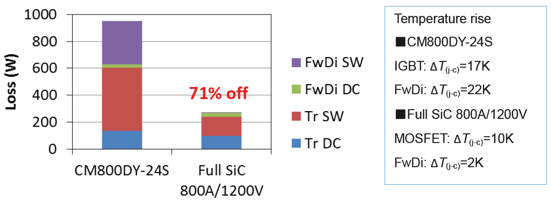
Figure 10: Loss and ΔT(j-c) simulation at fc=15kHz; VCC=600V; IO=400A(peak); PF=0,8; M=1,0
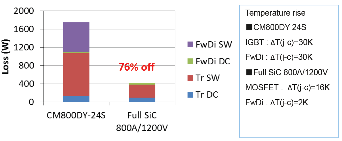
Figure 11: Loss and ΔT(j-c) simulation at fc=30kHz; VCC=600V; IO=400A(peak); PF=0,8; M=1,0
Gate Driver with SC-protection
The new 800A/1200V full SiC-Module can withstand a short circuit current for a limited time of tSC(max)=2,5μs. This limit is given in the SCSOA specification.
For conventional Si-IGBT modules typically a short circuit capability of tSC(max)=10μs is specified. In such conventional IGBT drivers a blanking time between desat-detection and SC-turn-off of typically to=1 3μs is installed, which is sufficient to ensure both: no false SC protection tripping and safe SC-turn-off.
Considering the relatively short tSC(max)=2,5μs specified for the new 800A/1200V full SiC-module another SC-protection method is proposed, known as RTC (Real Time Current Control). For this purpose one p-side and one n-side SiC MOSFET chip are equipped with a current sense electrode (refer to Figure 2). The equivalent circuit and the external view of this SiC MOSFET chip are shown in Figure 12.
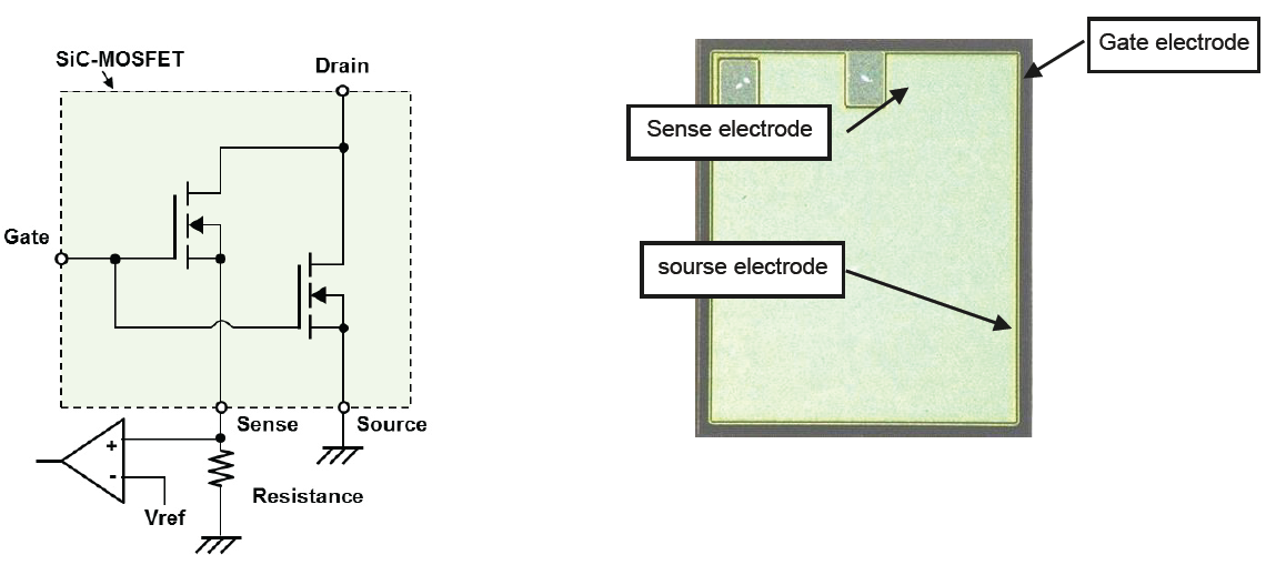
Figure 12: SiC MOSFET chip with current sense terminal
The functional block diagram of a dedicated gate driver for FMF800DX-24A using the proposed RTC protection is given in Figure 13. The measured short circuit waveforms during RTC operation are shown in Figure 14.
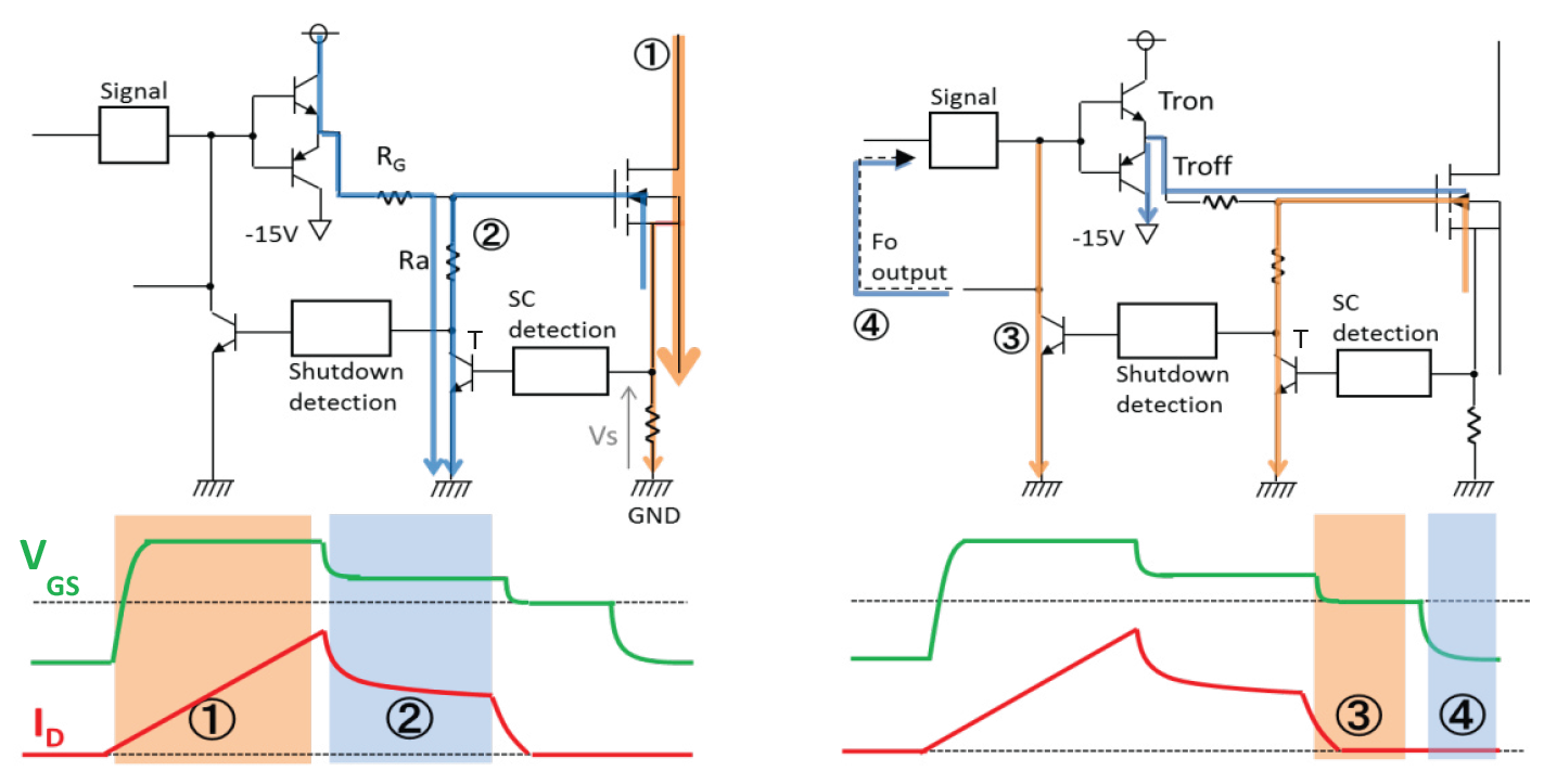
Figure 13: Principle of SC-protection by RTC
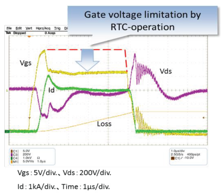
Figure 14: SC-waveforms during RTC-operation
During SC-turn-off operation by RTC four modes can be distinguished. In mode ① the main current ID is increasing until the voltage Vs across the shunt resistance is reaching a defined trip level. After reaching this trip level the mode ② starts: the transistor T is turned on and the Gate-Source voltage is reduced from +15V to about +7V resulting in a decreased SC-saturation current. Due to this SC-current reduction the allowable short circuit time is increased again to the well-known from IGBT drivers tsc(max)=10μs. Means from now on the conventional IGBT gate driver timing can be applied. During phase ③ the gate driver transistor Tron is switched off and VGS becomes Zero thus causing a soft turn-off of the short circuit current. In the final phase ④ the driver transistor Troff is turned on thus applying a negative VGS to the SiC MOSFET in off-state.
Summary and outlook
This paper is describing a new 800A/1200V full SiC dual module. Its type name is FMF800DX-24A. Compared with conventional Si-based IGBT modules the following unique points are confirmed:
- Module size reduced by 50%
- Switching loss (Esw=Eon + Eoff + Err) reduced by 75%
- Reliable SC-protection by RTC
Based on these features the new 800A/1200V full SiC module provides an interesting alternative to conventional IGBT modules in power electronic systems up to several 100kW, especially if one of the following system characteristics is of specific importance:
- Compact equipment size/high power density
- High efficiency
- High switching frequency (beyond the today’s limit reachable with IGBT modules)
References
[1]Press release No.2687 “Mitsubishi Electric to begin shipment of Silicon Carbide Power Modules Samples”, Tokyo, July 9, 2012
[2] Press release No.2733 “Mitsubishi Electric develops Large capacity SiC Power Module Technologies” Tokyo, February 14, 2013
Related posts
 Now available – DC/DC converters from PREMIUM
 New release in DACPOL lighting for lathes – Kira covers


Leave a comment