shopping_cart
Carro
0,00 PLN
0
Portapapeles
Debes estar logueado
-
-
-
Category
-
Semiconductores
- Diodos
- Tiristores
-
Módulos con aislamiento eléctrico
- Módulos con aislamiento eléctrico | VISHAY (IR)
- Módulos con aislamiento eléctrico | INFINEON (EUPEC)
- Módulos con aislamiento eléctrico | Semikron
- Módulos con aislamiento eléctrico | POWEREX
- Módulos con aislamiento eléctrico | IXYS
- Módulos con aislamiento eléctrico | POSEICO
- Módulos con aislamiento eléctrico | ABB
- Módulos con aislamiento eléctrico | TECHSEM
- Przejdź do podkategorii
- Rectificadores de puente
-
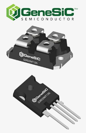
Transistores
- Transistores | GeneSiC
- Módulos SiC MOSFET | Mitsubishi
- Módulos SiC MOSFET | STARPOWER
- Módulos ABB SiC MOSFET
- Módulos IGBT | MITSUBISHI
- Módulos de transistores | MITSUBISHI
- Módulos MOSFET | MITSUBISHI
- Módulos de transistores | ABB
- Módulos IGBT | POWEREX
- Módulos IGBT | INFINEON (EUPEC)
- Elementos semiconductores de carburo de silicio (SiC)
- Przejdź do podkategorii
- Controladores de puerta
- Bloques de energía
- Przejdź do podkategorii
- Convertidores de corriente y tensión LEM
-
Componentes pasivos (condensadores, resistencias, fusibles, filtros)
- Resistencias
-
Fusibles
- Fusibles miniatura para circuitos electrónicos, serie ABC y AGC
- Fusibles tubulares de acción rápida
- Eslabones fusibles de retardo de tiempo con características GL / GG y AM
- Eslabones fusibles ultrarrápidos
- Fusibles de acción rápida (estándar británico y estadounidense)
- Fusibles de acción rápida (estándar europeo)
- Fusibles de tracción
- Eslabones fusibles de alto voltaje
- Przejdź do podkategorii
-
Condensadores
- Condensadores de motor
- Condensadores electrolíticos
- Condensadores de película
- Condensadores de potencia
- Condensadores para circuitos de CC
- Condensadores de corrección del factor de potencia
- Condensadores de alto voltaje
- Condensadores de calentamiento por inducción
- Condensadores de almacenamiento de energía y pulsos
- Condensadores de ENLACE CC
- Condensadores para circuitos AC/DC
- Przejdź do podkategorii
- Filtros EMI
- Supercondensadores
- Protección contra sobretensiones
- Filtros para detección de emisiones TEMPEST
- Pararrayos
- Przejdź do podkategorii
-
Relés y contactores
- Teoría de relés y contactores
- Relés semiconductores de CA trifásicos
- Relés semiconductores de CA trifásicos
- Reguladores, controles y accesorios
- Arranques suaves y contactores de inversión
- Relés electromecánicos
- Contactores
- Interruptores giratorios
-
Relés semiconductores de CA monofásicos
- Relés semiconductores CA monofásicos, serie 1 | D2425 | D2450
- Relés semiconductores CA monofásicos, series CWA y CWD
- Relés semiconductores CA monofásicos de las series CMRA y CMRD
- Relés semiconductores de CA monofásicos, serie PS
- Relés semiconductores de CA dobles y cuádruples, serie D24 D, TD24 Q, H12D48 D
- Relés de estado sólido monofásicos, serie gn
- Relés semiconductores de ca monofásicos, serie ckr
- Relés AC monofásicos SERIE ERDA Y ERAA para carril DIN
- Relés AC monofásicos para corriente 150A
- Relés dobles de estado sólido integrados con disipador de calor para carril DIN
- Przejdź do podkategorii
- Relés semiconductores CA monofásicos para PCB
- Relés de interfaz
- Przejdź do podkategorii
- Núcleos y otros componentes inductivos
- Radiadores, varistores, protecciones térmicas
- Aficionados
- Aire Acondicionado, Accesorios para Armarios Eléctricos, Neveras
-
Baterías, cargadores, fuentes de alimentación de búfer e inversores
- Baterías, cargadores - descripción teórica
- Baterías de iones de litio. Baterías personalizadas. Sistema de gestión de batería (BMS)
- Pilas
- Cargadores de baterías y accesorios
- Fuente de alimentación de respaldo de UPS y fuentes de alimentación de búfer
- Convertidores y accesorios para fotovoltaica
- Almacen de energia
- Celdas de combustible
- Baterías de iones de litio
- Przejdź do podkategorii
-
Automaticas
- Elevadores Spiralift
- Piezas para drones Futaba
- Finales de carrera, microinterruptores
- Sensores, transductores
- Pirometría
- Contadores, temporizadores, medidores de panel
- Dispositivos de protección industrial
- Señalización luminosa y sonora
- Cámara termográfica
- Pantallas LED
- Botones e interruptores
- Przejdź do podkategorii
-
Cables, alambres Litz, conductos, conexiones flexibles
- alambres
- Pasamuros y acopladores de cables
- cables Litz
-
Cables para aplicaciones especiales
- Los cables de extensión y compensación
- Cables para termopares
- Los cables de conexión a PT czyjnków
- Multicore cables temp. -60 ° C a + 1400 ° C
- cables de media tensión SILICOUL
- ignición alambres
- Los cables calefactores
- temp núcleo único. -60 ° C a + 450 ° C
- conductores de trenes
- El calentamiento de los cables en el Ex
- Przejdź do podkategorii
- camisas
-
trenzas
- trenzas planas
- trenzas ronda
- trenza muy flexible - plana
- trenza muy flexible - Ronda
- Copper cilíndrico trenzado
- Copper protector de la trenza y cilíndrica
- cintas de conexión flexibles
- Trenzas cilíndrico galvanizado y acero inoxidable
- Aislamiento de PVC trenzas de cobre - Temperatura 85 ° C
- aluminio trenzado plano
- Kit de conexión - trenzas y tubos
- Przejdź do podkategorii
- Accesorios para la tracción
- Terminales de cable
- barras flexibles aisladas
- carril flexible multicapa
- sistemas de gestión de cables
- Przejdź do podkategorii
- Zobacz wszystkie kategorie
-
Semiconductores
-
-
More Power and Higher Reliability by 7th Gen. IGBT Module with New SLC-Technology

More Power and Higher Reliability by 7th Gen. IGBT Module with New SLC-Technology
The main requirements of power electronics system are high efficiency, high power density and high reliability. To achieve the high efficiency Mitsubishi Electric developed the 7th Gen. IGBT chipset. To additionally fulfill the requirements of high reliability and high power density, the newly developed SLC package technology is combined with the 7th Gen Chip in the NX-type IGBT Modules Series.
By Thomas Radke, Mitsubishi Electric Europe B.V., Koichi Masuda, Mitsubishi Electric Corp., Japan
Industrial IGBT Modules are used in various fields of applications. All those applications require compact power modules with high power density, high reliability and high efficiency with reasonable cost. To fulfill all these requirements, the 7th Gen. NX-type IGBT Modules based on SLC-Technology have been developed. The 7th Gen. IGBT, which is based on CSTBT™ concept, provides high efficiency by the reduction of dynamic and static losses [2]. The loss reduction is the first step to realize a high power density module. In a second step the thermal resistance Rth must be improved in order to increase the power capability at a given operation temperature and to reduce the temperature swings. By combining improved temperature and power cycling capability, high reliability and compact power modules can be realized. The newly developed SLC-package technology provides low thermal resistance and high power and thermal cycling capability.
SLC-Technology
SLC (SoLid Cover) - Technology is a newly developed package technology for realizing high reliability and high thermal conductivity [3]. The comparison of the new package structure with a conventional structure is shown in Figure 1.
Metallized ceramic substrates are conventionally used to realize the electrical insulation between the electrical circuit with semiconductor chips and the module’s base plate. Those substrates are joint to the copper base plate by a solder layer. The drawback of this material combination is the mismatch of CTE (Coefficient of Thermal Expansion) between ceramics, solder and copper. This mismatch causes solder cracks by temperature swings and limits the life time of power modules. The module’s withstand capability against this stress is known as temperature cycling capability.
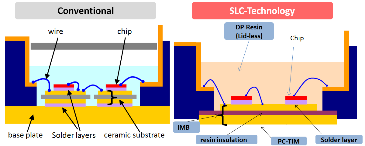
Figure 1: Comparison of SLC and conventional package structures
In the SLC-Technology the insulation is realized by a resin material which has a similar CTE value as copper. The base plate and the solder layer are eliminated because the top and bottom side copper layers can be directly bonded to the insulating resin layer. By this IMB (Insulated Metal Baseplate) the thermal cycling capability is essentially improved. Current status of the ongoing temperature cycle test is shown in Figure 2. Currently it has reached 40k cycles at 80K temperature swings. This result is about 7 times higher than the conventional capability, and this test is still ongoing without failure. Furthermore, as shown in the right side of Figure 2, after 40k cycles no delamination at all could be observed so far. Therefore even higher thermal cycling capability is expected.
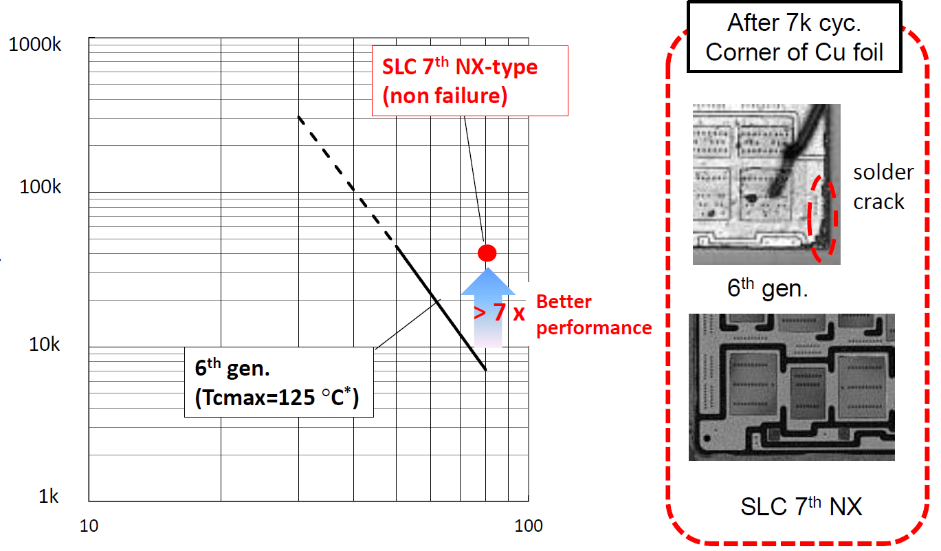
Figure 2: Thermal cycle test status
In conventional modules the maximum size of those ceramic substrates is limited by the thermal cycling capability because the mechanical stress applied to the solder layer caused by temperature swings is increasing with larger substrate size. Therefore in conventional IGBT Modules with a base plate size of 122mm x 62mm usually two or three ceramic substrates are used as shown in Figure 3. On the other hand the new SLC-technology consists of one common IMB owing to elimination of solder layer between substrate and baseplate. By this common substrate approach the effective area available for mounting power chips in the module is expanded and wire bond connections between the substrates are eliminated, thus reducing the internal parasitic package inductance and also the lead resistance. Hence the common IMB is one key element of the SLC-technology to achieve compact power modules with high power density.
Besides the thermal cycling capability also the power cycling capability must be considered to develop a high reliability power module. Main root cause of the power cycling failure mode is the degradation of the bonded wires joint. Continuously current flow and the related junction temperature swings cause strain at wire bonds. In the new SLC-technology the bondwires are covered by hard direct potting resin instead of soft silicone gel. By this hard DP-Resin, the mechanical stress of the wire bond is spread homogeneously to the whole surface of the wire as shown in Figure 4. In a conventional power module the mechanical stress of the wire is not absorbed so much by the soft silicone gel and that stress is concentrated to the base of the bonding wire. The 6th Gen. IGBT modules apply already an optimized and improved wire bonding technology to achieve the high power cycling life time with aluminum wires and soft silicone gel coat. Moreover by combination of this wire bonding technology and the SLC-technology the power cycling capability is essentially improved by keeping the well approved Aluminum wire bonds with their known cost advantages compared to expensive technologies like copper wire bonding. The comparison between the target power cycling capability of the SLCtechnology and the 6th Gen. modules is shown in Figure 5.
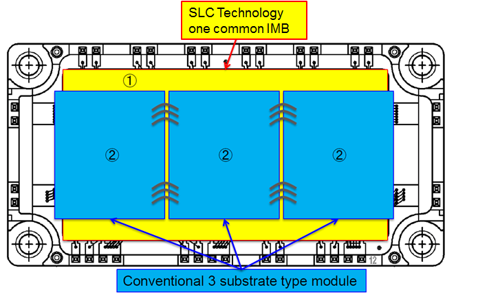
Figure 3: NX-type package with: 1 IMB and 2. Conventional ceramic substrate
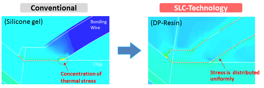
Figure 4: Stress concentration to the wire bond with Conventional and SLC-Technology
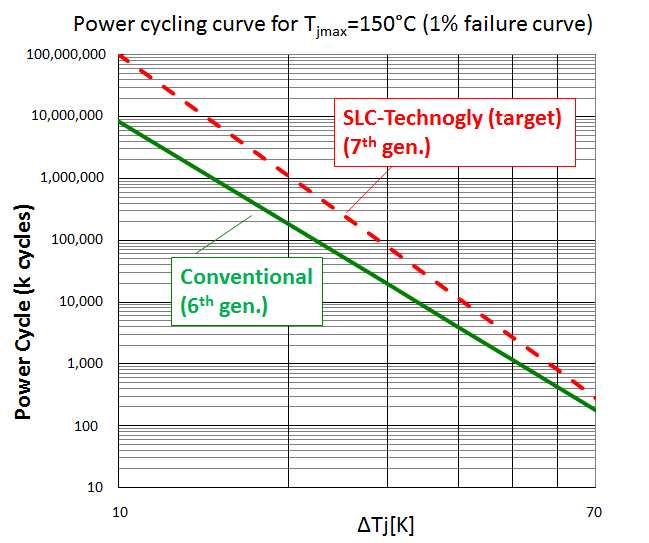
Figure 5: Power cycling capability of Conventional and SLC-Technology
To have a further improvement of the power cycling life time the junction temperature swing should be reduced. This can be achieved by improving the thermal resistance of the power module. Applications with constant load are usually thermally limited by the maximum junction temperature specification.
To cover also these requirements the SLC-technology has improved thermal resistances. SLC-technology applies the IMB, therefore the solder layer which has low thermal conductivity between substrate and baseplate is eliminated. The insulation material and the thickness of the insulation layer of the IMB are selected to achieve the best trade-off of insulation capability, reliability and low thermal resistance. By this optimization it is possible to achieve a reduction of the thermal resistance from junction to the case Rth(j-c) by approximately 30% compared to conventional modules where aluminum oxide (Al2O3) is widely used as ceramic material.
In conventional modules with copper baseplate and ceramics substrate, a warping of the baseplate also has to be considered during temperature cycles due to the unmatched CTEs and the resulting “bimetal effect”. This warping limits the possibility to improve the thermal contact resistance between baseplate and heat sink Rth(c-s). With the new SLC-technology which has the matched CTEs, this warping can be virtually eliminated and the thermal interface between baseplate and heat sink can be further improved by using an optimized pre applied phase change thermal interface material (PC-TIM). The total thermal resistance from junction to heat sink of a conventional module technology is about 43% higher than SLC-technology at same chip sizes. This outstanding thermal performance is also one of the essential features to fulfill the market requirements for high power density and high reliability.
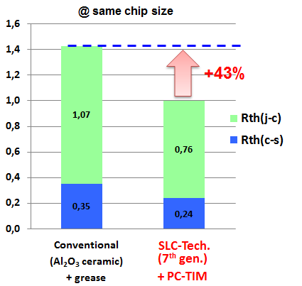
Figure 6: Comparison of thermal resistances at same chip size
7th Gen NX-type IGBT Modules
The new SLC-technology together with the 7th Gen IGBT chipset is introduced in the NX-type Modules Series of Mitsubishi Electric.
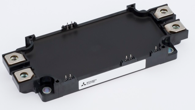
Figure 7: 7th gen NX-type 2in1 IGBT Module
The 7th Gen IGBT chip has an improved trade-off of collector emitter saturation voltage and turn-off switching losses. The cell design is optimized to have an improved controllability of the dv/dt by the gate resistor. By using the RFC structure (Relaxed Field of Cathode) for the freewheeling diode it is possible to improve also the trade-off of recovery losses and forward voltage drop by keeping the soft recovery behavior [2].
The characteristics of the new chip set was evaluated and used for the simulation of losses with the Mitsubishi simulation software called MELCOSIM [1]. The result is that the 1200V class 7th Gen IGBT can save about 15% of total losses compared to the 6th Gen IGBT under typical motor control inverter application conditions. To support the inverter assembly process on customer side, all 7th Gen. NX-type Modules will be available with the optimized PC-TIM and PressFit Pin terminals. Figure 8 shows that this NX-type 7th Gen IGBT Modules with SLC technology is underdevelopment with a comprehensive lineup to support wide range of applications with these new technologies.
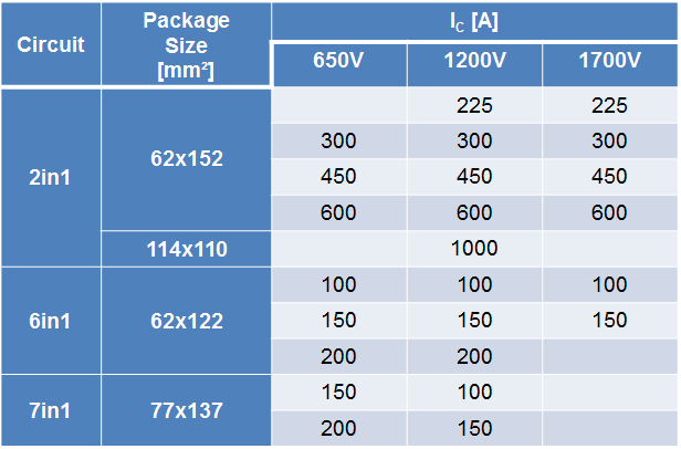
Figure 8: Line-up plan of 7th Gen NX-Type Modules with PC-TIM and PressFit options
System performance of 7th Gen Chipset and SLC-Technology
The features of 7th Gen Chipset from IGBT module point of view are explained. But to understand the impact on the inverter system these features have to be evaluated by a mission profile which is representative for typical inverter mode operation. For many applications load cycles have to be considered for the mission profile. By a loss simulation with the IGBT and diode chip characteristics this load profile can be transferred into a loss profile. From this loss profile with the thermal impedance the temperature profile can be calculated. Finally the lifetime can be predicted with the temperature profile in combination with the cycling capability curves from the modules [4].
In Figure 9, an example with normalized values is shown. From loss simulation by MELCOSIM it is noted that the total losses of 7th Gen. Chipset can be reduced by 15% compared to previous generation. It means the loss profile is reduced to 85%. As considering this 15% loss reduction and the approx. 30% improvement of the thermal resistance the junction Tj swings can be reduced to 60% compared to conventional module with aluminum oxide ceramics substrate and copper baseplate. In case of applying same loss that Tj swings of conventional module is 50K, Tj swings of SLC-Technology with 7th Gen. chipset would be 30K. So the result of target power cycling curves with the reduced Tj swings is that more than 10 times higher lifetime compared to conventional module can be reached by using the SLC-Technology with combination of 7th Gen IGBT. Or in case of the same life time the Tj swings with SLC-technology can be increased to about 57K which is equivalent to increased output power by more than 50%.
Summary
A new series of Mitsubishi IGBT modules for 600V and 1200V rated voltage has been developed covering a wide current range based on the well-established NX-package style. The new IGBT module series combines the latest 7th generation IGBT- and FWDi-chips with an innovative packaging technology, called SLC-technology. The new IGBT module series is enabling inverter designs with higher output currents, higher power density and improved reliability (increased power cycling life and increased temperature cycling life). It’s an excellent answer to the complex needs of state of the art inverter designs.
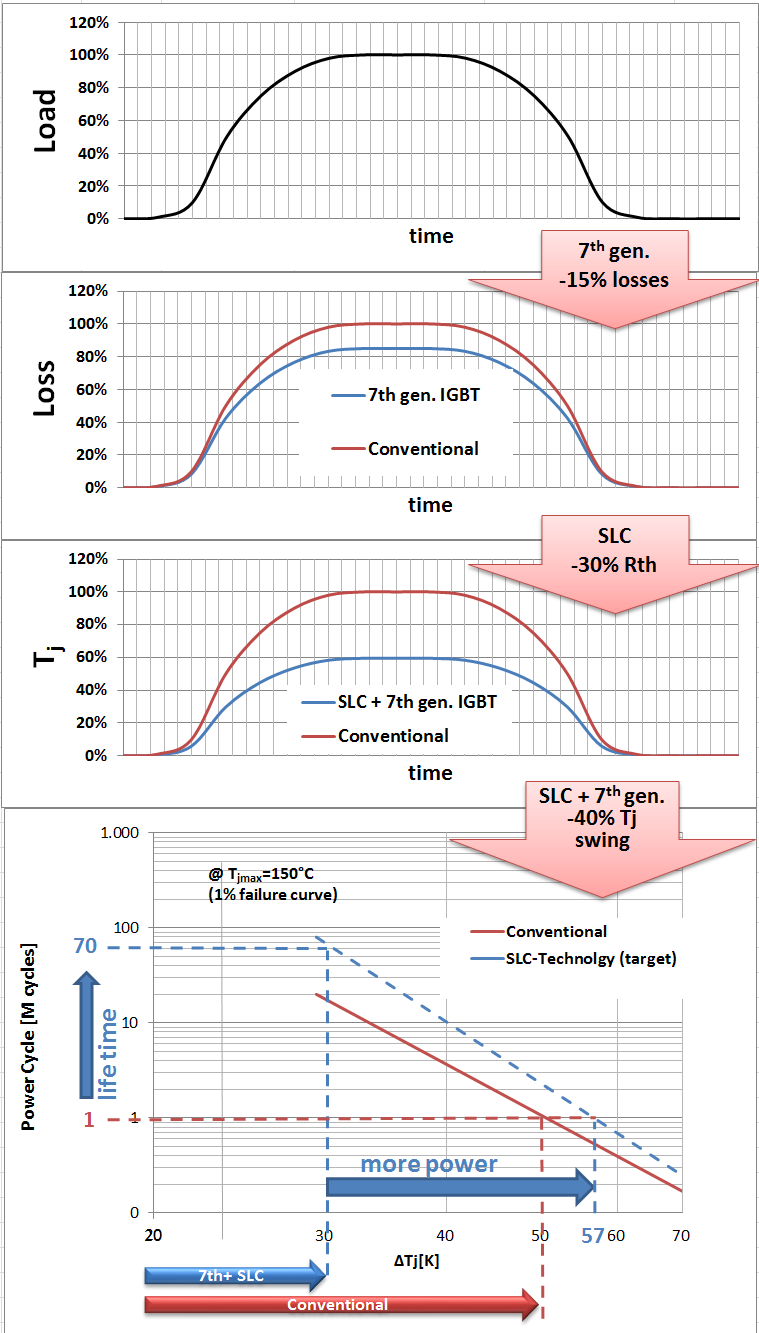
Figure 9: Normalized load cycle example with comparison of SLCtechnology with 7Gen. IGBT and Conventional Module
References
[1] MELCOSIM: IGBT thermal and loss simulation software, available at www.mitsubishielectric.com/semiconductors/simulator/
[2] T. Radke; K. Masuda: “7th Gen. IGBT and Diode Chip-set Enabling Highest Performance Power Modules”, Bodo’s Power Systems June 2015, page 42-35
[3] Kota Ohara, et al: “A New IGBT Module with Insulated Metal baseplate (IMB) and 7th Generation Chips” , PCIM Europe 2015, page 1145-1148, ISBN 978-3-8007-3924-0
[4] 6.1th Gen S1 Series NX-Type Application Note, available at www.mitsubishielectric.com/semiconductors/files/manuals/igbt_ nx_note_e.pdf
Publicaciones relacionadas
Now available – DC/DC converters from PREMIUM
We introduced a novelty to our permanent offer in DACPOL in the category of power supplies and converters and today...
Read more
New release in DACPOL lighting for lathes – Kira covers
We introduce a new product into the DACPOL category of industrial lighting and today we offer KIRA covers for...
Read more
Deja un comentario