Vous devez être connecté
-
WróćX
-
Composants
-
-
Category
-
Semi-conducteurs
- La diode
- Les thyristors
- Modules de puissance isolés
- Ponts redresseurs
-
Transistors
- Transistors | GeneSiC
- Modules MOSFET SiC | Mitsubishi
- Modules MOSFET SiC | STARPOWER
- Modules MOSFET SiC ABB
- Modules IGBT | MITSUBISHI
- Modules de transistors | MITSUBISHI
- Modules MOSFET | MITSUBISHI
- Modules de transistors | ABB
- Modules IGBT | POWEREX
- Modules IGBT | INFINEON (EUPEC)
- Composants semiconducteurs en carbure de silicium
- Przejdź do podkategorii
- Circuits de commande
- Blocs de puissance
- Przejdź do podkategorii
- Transducteurs électriques
-
Composants passifs (condensateurs, résistances, fusibles, filtres)
- Résistances
-
Fusibles
- Fusibles miniatures pour c.imp. série ABC et AGC
- Fusible rapides tubulaires
- Cartouches de courbe GL/GG et AM
- Cartouches ultrarapides
- Fusibles à action rapide (norme britannique et américaine)
- Fusibles à action rapide (norme européenne)
- Fusibles de traction
- Cartouche de haute tension
- Przejdź do podkategorii
-
Condensateurs
- Condensateurs pour moteurs
- Condensateurs électrolitiques
- Condensateurs de type snubbers
- Condensateurs de puissance
- Condensateurs pour circuits continus
- Condensateurs de compensation de puissance
- Condensateurs de haute tension
- Condensateurs pour chauffage par induction
- Condensateurs pour impulsions
- Condensateurs DC LINK
- Condensateurs pour circuits AC/DC
- Przejdź do podkategorii
- Filtres anti-interférences
- Supercondensateurs
- Protection contre les surtensions
- Filtres de détection des émissions TEMPEST
- Przejdź do podkategorii
-
Relais et contacteurs
- Théorie relais et contacteurs
- Relais statiques triphasés
- Relais statiques CC
- Régulateurs, circuits de commande et accessoires
- Démarrages progressifs et contacteurs inverseurs
- Relais electromécaniques
- Contacteurs
- Commutateurs rotatifs
-
Relais statiques monophasés
- Relais semi-conducteurs AC monophasés, série 1 | D2425 | D2450
- Relais à semi-conducteurs CA monophasés, séries CWA et CWD
- Relais à semi-conducteurs CA monophasés des séries CMRA et CMRD
- Relais à semi-conducteurs CA monophasés, série PS
- Relais semi-conducteurs AC double et quadruple, série D24 D, TD24 Q, H12D48 D
- Relais statiques monophasés, série GN
- Relais à semi-conducteurs CA monophasés, série CKR
- Relais AC monophasés SÉRIES ERDA ET ERAA pour rail DIN
- Relais CA monophasés pour courant 150A
- Relais à semi-conducteurs doubles intégrés à un dissipateur thermique pour un rail DIN
- Przejdź do podkategorii
- Relais statiques monophasé pour c.imp.
- Relais d'interface
- Przejdź do podkategorii
- Composants inductifs
- Radiateurs, varistances, protections thermiques
- Ventilateurs
- Climatiseurs et accessoires d'armoires électriques
-
Batteries, chargeurs, blocs d'alimentation tampon et onduleurs
- Batteries et Chargeurs - théorie
- Batteries Li-ion et non-standards. Systèmes de gestion des batteries (BMS)
- Batteries
- Chargeurs de batteries et accessoires
- Alimentation de secours UPS et alimentation tampon
- Convertisseurs de tension et accessoires pour photovoltaïque
- Stockage d'Energie
- Réservoirs de carburant
- Batteries lithium-ion
- Przejdź do podkategorii
-
Automatique industrielle
- Élévateurs Spiralift
- Pièces pour drones Futaba
- Interrupteurs de fin de course, micro-rupteurs
- Capteurs et convertisseurs
- Pyromètres
- Compteurs, Relais temporisés, Indicateurs de tableau
- Appareils industriels de protection
- Signalisation lumineuse et sonore
- Caméra thermique
- Afficheurs à LED
- Boutons et commutateurs
- Przejdź do podkategorii
-
Câbles et chemins de câbles
- Fils
- Passe-câbles et coupleurs
- Fils de Litz
- Câbles pour les applications spéciales
- Gaines
-
Tresses
- Tresses plates
- Tresses rondes
- Tresses très souples - plates
- Tresses très souples - rondes
- Tresses cuivre cylindriques
- Tresses cuivre cylindriques et protection
- Bandes de mise à la terre souples
- Tresses en acier zingué et inox
- Tresses isolantes en PVC - temp. 85°C
- Tresses plates en aluminium
- Kit de liaison - tresses et gaines
- Przejdź do podkategorii
- Equipement pour la traction
- Cosses
- Barres flexible isolées
- Barre flexibles multicouches
- Systèmes de traçage des câbles
- Przejdź do podkategorii
- Zobacz wszystkie kategorie
-
Semi-conducteurs
-
-
- Fournisseurs
-
Applications
- Alimentations (UPS) et systèmes de redressement
- Automatisation HVAC
- Automatisation industrielle
- Chauffage par induction
- Composants pour atmosphères potentiellement explosives (EX)
- Dispositifs de protection industriels
- Énergétique
- Energy bank
- Équipements pour armoires de distribution, de contrôle et de télécommunications
- Impression
- Machines à souder et machines à souder
- Machines de séchage et de traitement du bois
- Machines pour le thermoformage des plastiques
- Machines-outils CNC
- Mesure et régulation de la température
- Mesure et régulation de la température
- Mines, métallurgie et fondation
- Moteurs et transformateurs
- Traction de tram et de chemin de fer
- Variateurs CA et CC (onduleurs)
-
Installation
-
-
Inducteurs
-
-
Appareils à induction
-
-
Service
-
- Contact
- Zobacz wszystkie kategorie
New Transfer Molded SMD Type IPM

New Transfer Molded SMD Type IPM
Mitsubishi Electric has added a new transfer molded SMD type Intelligent Power Module to its line-up – the MISOP™. The MISOP™ is an ideal solution for high performance inverters in the range of 100W which require a high degree of compactness, high efficiency and easy assembly.
By Narender Lakshmanan and Muzaffer Albayrak from Mitsubishi Electric Europe B.V, Germany Teruaki Nagahara, Mitsubishi Electric Power Device Works, Japan
Introduction
Applications such as small drives (in the range of 100W output power) have certain special requirements with regards to the design of the power supply unit. The power supply unit encompasses the power semiconductor module and the associated peripheries (such as gatedrive, control, protection and heatsink) which are assembled using a single PCB. This unit must be able to deliver the highest possible efficiency and must offer a high degree of compactness. Additionally, it is expected that the modules must be mounted with minimum effort on the PCB. Considering the special requirements presented by such applications, the MISOP™ (Mitsubishi Electric Intelligent Small Outline Power Module) are being developed in the 1A/600V range and the 3A/600V range. The MISOP™ is SMD type Intelligent Power Module (IPM) which consists of integrated gate-driver components and bootstrap diodes.
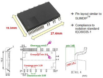
Figure 1 : Package dimensions of the MISOP™ and the pin layout indicating the compliance to the IEC60335-1
This product is a new addition in the Mitsubishi DIPIPM™ family of products which consist of transfer molded power semiconductors optimized for applications requiring a high degree of compactness and high operational efficiency.
Highly Optimized SMD type Power module:
The MISOP™ is based on the Mitsubishi 7th generation Reverse Conduction (RC) IGBT chip technology. The 7th generation chip technology is a low loss thin wafer IGBT technology which allows an optimization of the balance between performance and IGBT chip size. In addition to the inherent benefits of the 7th generation chip technology, the RC technology enables a significant level of optimization of the power module’s surface area requirement since the IGBT and the diode are effectively integrated into a single die. As a result, the chip surface which is normally used for the placement of diode dies are not required in this approach and therefore the IGBTs and the diodes necessary for a 3 phase inverter are effectively packed into a single package corresponding to the SOP footprint. Figure 1 indicates the size of the package and Figure 2 indicates the internal circuit topology of the power module. The pin assignment is similar to that of Mitsubishi’s SLIMDIP™ module from the DIPIPM™ series and the isolation standard has been designed under the consideration of market requirements of creepage and clearance distances.
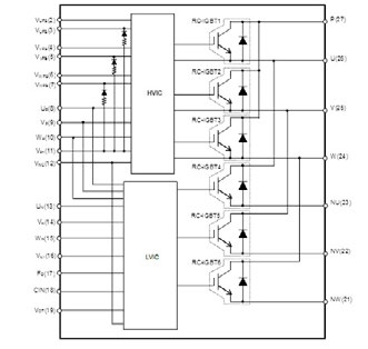
Figure 2 : The internal topology of the MISOP™
Pin design is also in accordance with the norm IEC60335-1. This product has been developed in the SMD package. It does not have throughhole pins and it can be soldered to the PCB using the reflow soldering technique which is intended to optimize efforts required in the assembly process. Continuing with the concept of the DIPIPMTM series, the MISOP™ is also equipped with integrated gate drive components. The module is equipped with embedded driver ICs: a Low Voltage IC (LVIC) which is responsible for driving the low side switches and a High Voltage IC (HVIC) which utilizes the bootstrap topology to drive the high side switches (with bootstrap diodes and current limiting resistors). The full integration of driver and protection functionality are guaranteed under Mitsubishi quality standards and allows to reduce the failure rate of whole inverter. Also, through the full integration, the number of peripheral components will be optimized and this would help the stock management. The embedded gate drive ICs also support several important protection functionalities. Figure 3 indicates the wiring pattern which has to be established in an application utilizing the MISOP™. The approach adopted by the MISOP™ avoids the needs for several undesirable cross points in the PCB tracks and even enables to use a single-side board. As a result, the PCB board design required for utilizing the MISOP™ is significantly simplified.
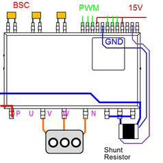
Figure 3: An example of the application circuit required for MISOP™ indicating the connections to the shunt resistors, Bootstrap-Capacitors, control input, control power supply and power terminals.
Performance Analysis
The increasing global awareness for carbon footprint reduction combined with the commercial benefit of reducing power consumption in appliances has motivated manufacturers of inverters (for applications such as small fans or pumps) in the range of 100W output power to adopt power semiconductors which deliver the highest possible efficiency during operation. Therefore, along with the advantage of offering compactness and easy design, the MISOP™ must be able to perform well under the required operating conditions. Figure 4 indicates simulation results of the power loss performance with the 1A device MISOP™ for different RMS inverter current Iout(rms) and the corresponding increase in the ΔTj-c(average) for the given values of the Iout(rms). Considering an inverter with the following nominal working conditions: Iout = 0.283 Arms, Vcc = 300V, fc = 20 kHz, pf = 0.8, modulation index = 1; the 3 phase output power is approximately 72W by using the 1A devices (SP1SK) from MISOP™ family. Using the data from Figure 4, we understand that the total power loss is around 2.76W. This performance indicates a power module efficiency of around 96%. Although the MISOP™ is highly compact in volume, it can be observed that this module is capable of delivering excellent thermal performance. With regards to the thermal performance, it is evident that the ΔTj-c(average) for this operating point is around 7 K for each RC-IGBT. Under these operating conditions, (considered an air cooled heatsink with effective Rthc-s =16 K/W for the entire module and ambient temperature of around 40°C) the temperature of the case remains at around 85°C and the average junction temperature remains at around 92°C. Figure 5 indicates the thermal performance of the module captured via a thermal camera (this analysis was performed without any external heatsink). A combination of high operational efficiency and good thermal performance enables the inverter to achieve maximum output power from this MISOP module.
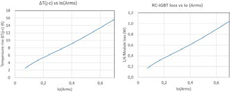
Figure 4: Tentative data pertaining to the thermal and electrical loss performance of a single RC-IGBT device (MISOP™). Conditions: Vcc = 300V, fc = 20 kHz, pf = 0.8, M = 1, Three Phase Modulation, Rth(j-c) maximum, Tj = 125°C, heatsink connected.
Integrated Protection Functions
Along with the requirement for high efficiency, it also necessary to ensure that the inverter is designed using a high performance power module with regards to protection against irregular operation modes. The MISOP™ is provided with several integrated protection functions (please refer to Table 1). The device offers the possibility to implement a short circuit protection via external shunt resistances which can be connected to each of the open emitter pins. To avoid the risk of overheating during operation, there is a built-in overtemperature protection function (OT) and there is a possibility of monitoring the module temperature with an accurate linear analog voltage output signals (VOT), which could help to define the derating points to use the module with high power density. The availability of the “interlock-protection” is an important implementation, this protection function prevents the simultaneous turn-on of both high side and low side switches (such a turn-on would lead to an arm-shot through short circuit). In addition, there is a system to detect and indicate a failure in the control supply voltage. An unstable input to the control power supply can lead to undefined switching states and subsequently thermal run-away of power chips. A failure event in any of the low side switches would be indicated via the Fo signal (except for interlock function).
| # | Functions available in the MISOP™ |
|---|---|
| 1 | Under voltage protection (UV) |
| 2 | Short circuit Protection (SC) |
| 3 | Over temperature protection (OT) |
| 4 | Temperature information output (VOT) |
| 5 | Arm short circuit protection -> Interlock (IL) |
| 6 | Failure output (Fo) |
| 7 | Bootstrap diode (BSD) |
| 8 | Open emitter N side :Three shunts can be connected |
Table 1 : List of internal functionalities available in the MISOP™
Summary
Indices such as the APF (Annual Performance Factor) pertaining to efficiency have gained significance in recent years and have motivated the manufacturers of appliances such as small fans, pumps and various other such appliances which require an output power in the range of 100W to consider power semiconductor devices which offer high operational efficiencies. Simultaneously, the demand for inverter size optimization has led to the demand for highly optimized power modules. On the other hand, such a compact power module must also be robust and offer high reliability. The MISOP™ is designed to address the requirements of this sector. In addition to the availability of integrated functionalities (such as protection functions), the MISOP™ package allows for easy and efficient assembly process. In addition, it must also be noted that the wiring scheme required for the MISOP™ facilitates an easy PCB design thanks to similar pin layout with Mitsubishi’s SLIMDIP™ module and the secured pin to pin isolation distance in accordance with isolation standard IEC60335-1.

Figure 5: Heatsink-less operation captured using a thermal camera Vcc=270V, VD=15V, Io=0.12 and 0.28Arms, fc=16kHz, Modulation= 1, Three phase sine wave, Natural convection (no forced air), Ta=20.9~21.6ºC, Evaluation board, typical data.
References
[1] The DIPIPM™ family concept http://www.mitsubishielectric.com/semiconductors/products/powermod/dipipm/index.html
[2] Datasheet – SLIMDIP Module: http://www.mitsubishielectric.com/semiconductors/content/product/powermodule/dipipm/slimdip/slimdip-s_e.pdf
[3] Press release: Mitsubishi Electric to Launch MISOP Surfacemount Package IPM http://de.mitsubishielectric.com/de/newsevents/releases/global/2018/0416-a/index.page
Articles similaires
 Now available – DC/DC converters from PREMIUM
 New release in DACPOL lighting for lathes – Kira covers


Laissez un commentaire