shopping_cart
Chariot
0,00 PLN
0
Cache
Vous devez être connecté
-
-
-
Category
-
Semi-conducteurs
- La diode
- Les thyristors
- Modules de puissance isolés
- Ponts redresseurs
-
Transistors
- Transistors | GeneSiC
- Modules MOSFET SiC | Mitsubishi
- Modules MOSFET SiC | STARPOWER
- Modules MOSFET SiC ABB
- Modules IGBT | MITSUBISHI
- Modules de transistors | MITSUBISHI
- Modules MOSFET | MITSUBISHI
- Modules de transistors | ABB
- Modules IGBT | POWEREX
- Modules IGBT | INFINEON (EUPEC)
- Composants semiconducteurs en carbure de silicium
- Aller à la sous-catégorie
- Circuits de commande
- Blocs de puissance
- Aller à la sous-catégorie
- Transducteurs électriques
-
Composants passifs (condensateurs, résistances, fusibles, filtres)
- Résistances
-
Fusibles
- Fusibles miniatures pour c.imp. série ABC et AGC
- Fusible rapides tubulaires
- Cartouches de courbe GL/GG et AM
- Cartouches ultrarapides
- Fusibles à action rapide (norme britannique et américaine)
- Fusibles à action rapide (norme européenne)
- Fusibles de traction
- Cartouche de haute tension
- Aller à la sous-catégorie
-
Condensateurs
- Condensateurs pour moteurs
- Condensateurs électrolitiques
- Condensateurs de type snubbers
- Condensateurs de puissance
- Condensateurs pour circuits continus
- Condensateurs de compensation de puissance
- Condensateurs de haute tension
- Condensateurs pour chauffage par induction
- Condensateurs pour impulsions
- Condensateurs DC LINK
- Condensateurs pour circuits AC/DC
- Aller à la sous-catégorie
- Filtres anti-interférences
- Supercondensateurs
-
Protection contre les surtensions
- Protection contre les surtensions pour les applications coaxiales
- Protection contre les surtensions pour les systèmes de vidéosurveillance
- Parafoudres de ligne électrique
- Protection contre surtensions pour LED
- Parafoudres pour le photovoltaïque
- Protection du système de pesage
- Protection contre les surtensions pour bus de terrain
- Aller à la sous-catégorie
- Aller à la sous-catégorie
-
Relais et contacteurs
- Théorie relais et contacteurs
- Relais statiques triphasés
- Relais statiques CC
- Régulateurs, circuits de commande et accessoires
- Démarrages progressifs et contacteurs inverseurs
- Relais electromécaniques
- Contacteurs
- Commutateurs rotatifs
-
Relais statiques monophasés
- Relais semi-conducteurs AC monophasés, série 1 | D2425 | D2450
- Relais à semi-conducteurs CA monophasés, séries CWA et CWD
- Relais à semi-conducteurs CA monophasés des séries CMRA et CMRD
- Relais à semi-conducteurs CA monophasés, série PS
- Relais semi-conducteurs AC double et quadruple, série D24 D, TD24 Q, H12D48 D
- Relais statiques monophasés, série GN
- Relais à semi-conducteurs CA monophasés, série CKR
- Relais AC monophasés SÉRIES ERDA ET ERAA pour rail DIN
- Relais CA monophasés pour courant 150A
- Relais à semi-conducteurs doubles intégrés à un dissipateur thermique pour un rail DIN
- Aller à la sous-catégorie
- Relais statiques monophasé pour c.imp.
- Relais d'interface
- Aller à la sous-catégorie
- Composants inductifs
- Radiateurs, varistances, protections thermiques
- Ventilateurs
- Climatiseurs et accessoires d'armoires électriques
-
Batteries, chargeurs, blocs d'alimentation tampon et onduleurs
- Batteries et Chargeurs - théorie
- Batteries Li-ion et non-standards. Systèmes de gestion des batteries (BMS)
- Batteries
- Chargeurs de batteries et accessoires
- Alimentation de secours UPS et alimentation tampon
- Convertisseurs de tension et accessoires pour photovoltaïque
- Stockage d'Energie
- Réservoirs de carburant
- Batteries lithium-ion
- Aller à la sous-catégorie
-
Automatique industrielle
- Futaba Drone Parts
- Interrupteurs de fin de course, micro-rupteurs
- Capteurs et convertisseurs
- Pyromètres
- Compteurs, Relais temporisés, Indicateurs de tableau
- Appareils industriels de protection
- Signalisation lumineuse et sonore
- Caméra thermique
- Afficheurs à LED
- Boutons et commutateurs
-
Enregistreurs
- Enregistreur de température à bande et afficheur numérique - AL3000
- Enregistreurs à microprocesseur avec ecran LCD série KR2000
- Enregistreur KR5000
- Indicateur avec fonction enregistrement de température et humidité HN-CH
- Matériaux consommables pour enregistreurs
- Enregistreur graphique compact 71VR1
- Enregistreur KR3000
- Enregistreur PC série R1M
- Enregistreur PC série R2M
- Enregistreur PC, 12 entrés isolées – RZMS
- Enregistreur PC, USB, 12 entrées isolées – RZUS
- Aller à la sous-catégorie
- Aller à la sous-catégorie
-
Câbles et chemins de câbles
- Fils
- Fils de Litz
- Câbles pour les applications spéciales
- Gaines
-
Tresses
- Tresses plates
- Tresses rondes
- Tresses très souples - plates
- Tresses très souples - rondes
- Tresses cuivre cylindriques
- Tresses cuivre cylindriques et protection
- Bandes de mise à la terre souples
- Tresses en acier zingué et inox
- Tresses isolantes en PVC - temp. 85°C
- Tresses plates en aluminium
- Kit de liaison - tresses et gaines
- Aller à la sous-catégorie
- Equipement pour la traction
- Cosses
- Barres flexible isolées
- Barre flexibles multicouches
- Systèmes de traçage des câbles
- Gaines annelées, tuyaux
- Aller à la sous-catégorie
- Voir toutes les catégories
-
Semi-conducteurs
-
-
Enhanced Power Density and Expanded Line-up of the 7th Gen Industrial IGBT Modules Utilizing the Improved Thermal Conductivity of the Highly Reliable SLC-Technology

Enhanced Power Density and Expanded Line-up of the 7th Gen Industrial IGBT Modules Utilizing the Improved Thermal Conductivity of the Highly Reliable SLC-Technology
The 7th gen. Industrial IGBT modules have been successfully developed for the 650V and the 1200V classes to cover important power electronics system requirements such as high efficiency, high power density and high reliability. The outstanding results pertaining to the thermal cycling capability, the “pumping out failure” free package and the low thermal resistance of the SLC-Technology in combination with the low loss 7th generation chipsets are the key reasons for the success of the 7th gen NX-type IGBT modules. To expand this technology to the 1700V class IGBT modules, the insulation capability and the thermal conductivity of the SLC-Technology’s IMB has been improved. By Thomas Radke and Narender Lakshmanan, Mitsubishi Electric Europe B.V. and Takuya Takahashi and Shinsuke Asada, Mitsubishi Electric Corporation Japan, Power Device Works
By Thomas Radke and Narender Lakshmanan, Mitsubishi Electric Europe B.V. and Takuya Takahashi and Shinsuke Asada, Mitsubishi Electric Corporation Japan, Power Device Works
Introduction
The 7th gen. 650V and 1200V class Industrial IGBT modules have been introduced recently to the market. In this new IGBT module generation, the latest chip technology has been utilized [1] to cover the requirements of industrial power electronics applications. All those applications utilize the superior characteristics of the 7th gen NX-Type IGBT modules which are - compactness, high power density, high reliability, high efficiency and reasonable cost [2]. To expand the area of applicability to the 1700V class modules, the IMB (Insulated Metal Baseplate) which is a key element of the SLC-Technology has been improved.
SLC-Technology with high thermal conductivity and insulation properties
Generally, Al2O3 substrates are often used as the insulating layer in power modules. However, Mitsubishi Electric has employed the Aluminum Nitride (AlN) substrate in the previous generations e.g. 5th and 6th gen. IGBT modules. Due to the superior thermal conductivity achieved by using AlN instead of Al2O3 the total thermal resistance Rth(j-c) between the chip and the baseplate was reduced by about 35%, see Figure 1
However, it is difficult to improve the thermal conductivity of ceramic any further. In addition, there is a stress experienced at the interconnection between the ceramic layer and the metal layer during thermal cycling due to the mismatch of CTE (Coefficient of Thermal Expansion) between these materials as shown in Table. 1. However, employing thinner ceramic substrates with the aim of improving the thermal resistance is not always the best approach. The thinner the substrate, the more sensitive it becomes against damages as a result of mechanical stresses. To address this problem, the SLC-Technology with the IMB structure has been developed [3]. A cross section of this new structure is shown in Figure 2,
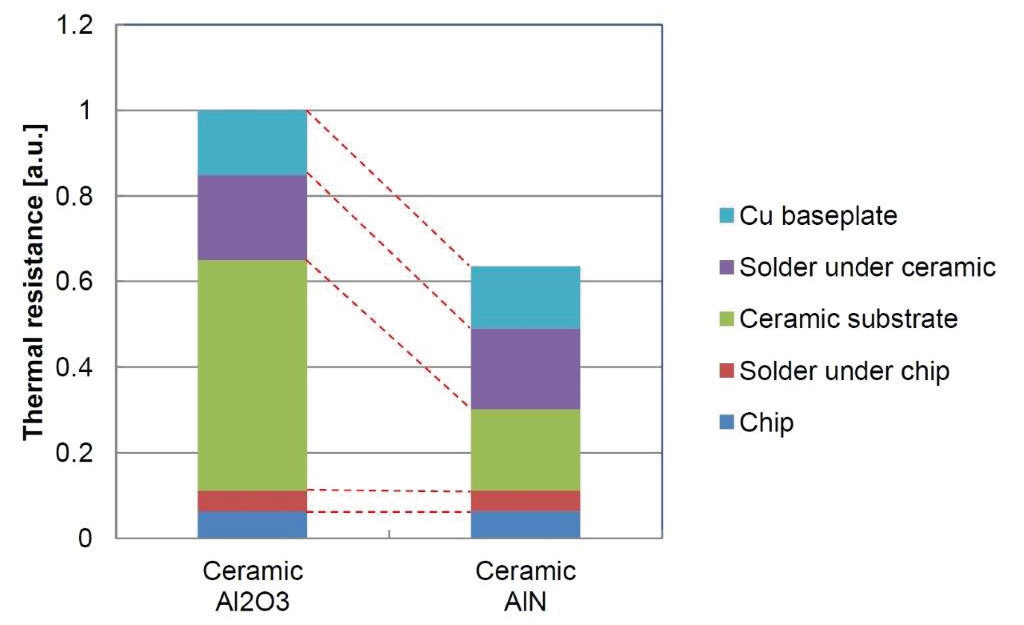
Figure 1: Simulation result of thermal resistance Rth(j-c)
By selecting the CTE-value of the IMB’s insulating resin layer to be close to the CTE-values of the top and bottom metal layers, the mechanical stress caused by the mismatch of the CTE-values is reduced.
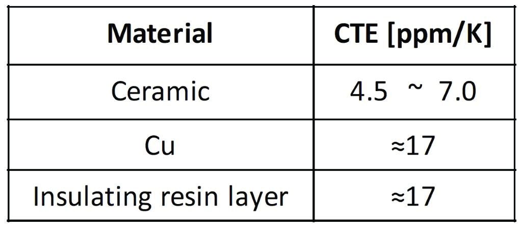
Table 1: Coefficients of Thermal Expansion CTE
Therefore, in comparison with the conventional structure using ceramic isolation substrates, the thickness of the insulating layer in the IMB can be reduced and the thickness of the metal layers can be increased respectively. By this approach, a thick metal layer can be chosen at the bottom side, thereby substituting the metal baseplate and eliminating the large solder layer area between baseplate and the ceramic substrate which is typical for conventional modules. As a result, the thermal resistance and the thermal cycling capability can be improved.
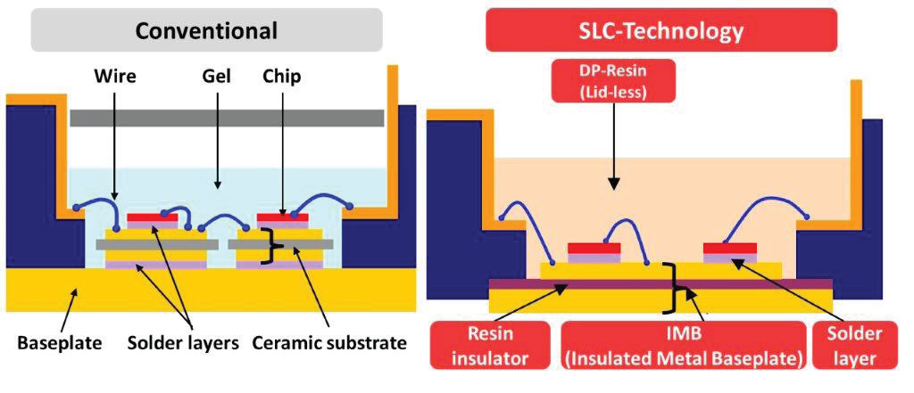
Figure 2: Package structure of conventional and new 7th gen NX-type IGBT module with SLC-technology
Furthermore, compared to the surface area available for chip mounting at ceramic substrates, the surface area of the newly developed IMB can be enlarged because the size limitation known for ceramic substrates does not exist for IMB. Eliminating this size limitation provides flexibility in designing the size and the shape of the IMB. As result a higher chip mounting density in the module can be achieved by eliminating the interconnecting wires between the multiple isolation substrates. In addition, the thickness of the topside metal layer can be increased resulting in a reduction of the electrical lead resistance. This allows for designing the top side metallization pattern with narrower current traces, which helps in further increasing the area available for chip mounting and thereby increasing the power density in the module.
A second positive result obtained by employing an increased thickness of the topside metal layer is associated with the heat spreading effect which in-turn facilitates a further reduction in the thermal resistance “Rth(j-c)” and a reduction in the transient thermal impedance “Zth(j-c)” by virtue of the enhanced thermal capacity.
Optimization of the properties of the IMB for higher isolation voltage
The complete line-up of 7th gen NX-type IGBT modules is given in Table 2. The isolation voltage of 650V and 1200V class modules is specified as Viso=2,5kV AC 1min; for the 1700V class modules the isolation voltage is Viso=4kV AC 1min.
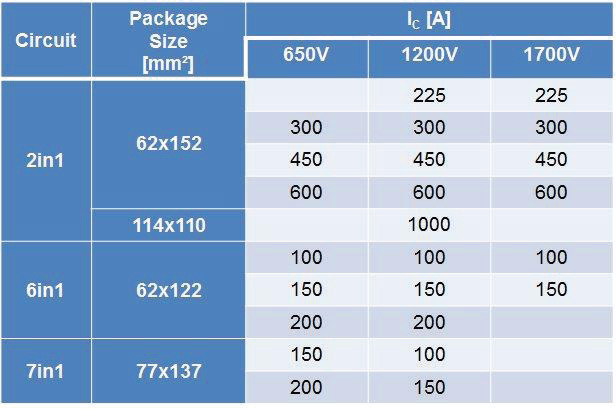
Table 2: Line-up of 7th gen NX-type IGBT modules
An example of module package is shown in Figure 3. The same package size (62mm x 152mm footprint) is used for the 600A 2in1 modules for all three voltage classes 650V, 1200V and 1700V. For reaching the same 600A rated module current at Vces=1700V and Viso=4kV in the same package size with 62mm x 152mm footprint, the IMB had to be improved. It was necessary to increase the specific thermal conductivity of the insulating resin layer in order to compensate the additional thickness of the insulating layer needed for Viso=4kV.
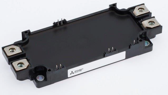
Figure 3: Package outline of 600A 2in1 NX-type IGBT module for 650V, 1200V and 1700V
The insulation layer of the IMB consists of resin and ceramic particles. To achieve an improvement in thermal conductivity, it is necessary to increase the area of the heat conducting path within the isolation layer (represented here by the ratio of the ceramic particles to the resin quantity, the higher the ceramic particles ratio, the better the thermal conductivity and vice versa). However, for a given fixed volume, if the ratio of ceramic particles to the resin quantity is increased, the quantity of resin shrinks. This reduced resin quantity results in lower viscosity and consequently hinders the productivity of the IMB manufacturing process. Further, if the ceramic particles volume concentration exceeds a critical value, the dielectric breakdown voltage capability decreases drastically. Thus, the quantity of ceramic particles, the resin quantity and the distribution of the ceramic particle size need to be carefully adjusted in order to achieve well-tuned trade-off characteristics of the isolation layer. By virtue of tailored resin material composition design and IMB manufacturing process optimization, it was possible to enhance both the thermal conductivity and the withstand voltage capability as reflected in the successful realization of the NXType 1700V class modules [3].
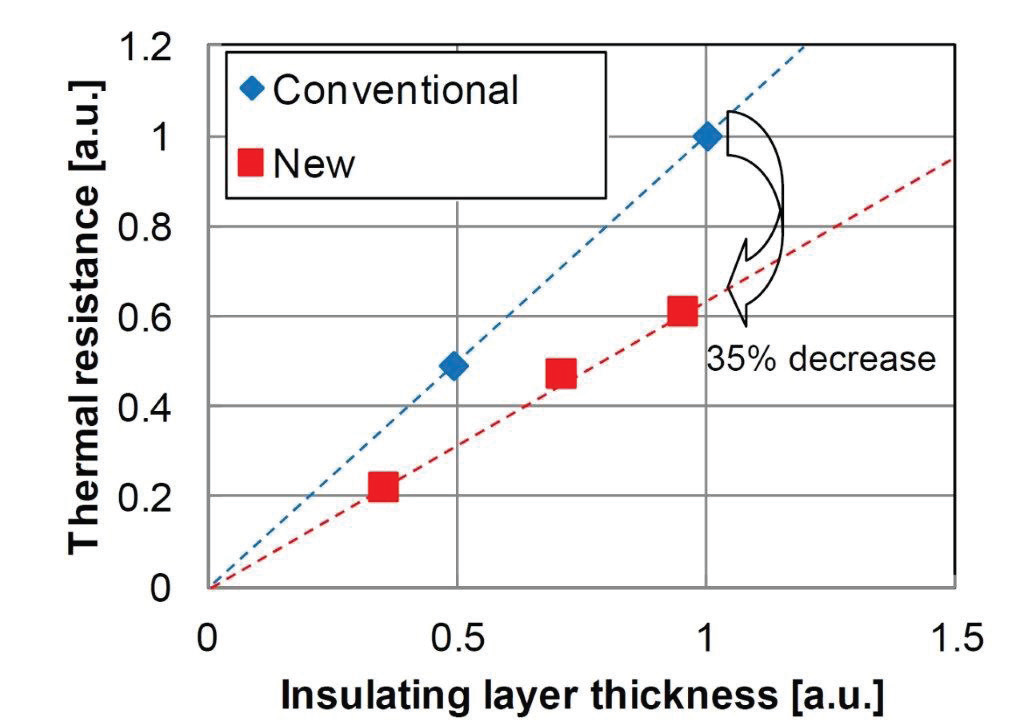
Figure 4: Measurements result of IMB thermal resistance with different thickness
Figure 4 shows the measurement result of the thermal resistance of the IMB versus the resin insulating layer thickness. The total thermal resistance of the IMB is approximately 35% better compared to the conventional IMB because the thermal conductivity of the resin insulation layer is enhanced by 50%. The new IMB’s partial discharge inception voltage (PDIV) shows almost the same dependency on layer thickness as the conventional IMB. Thus, the proposed IMB has been confi rmed to have equivalent PDIV and insulation characteristics while possessing an improved thermal conductivity.
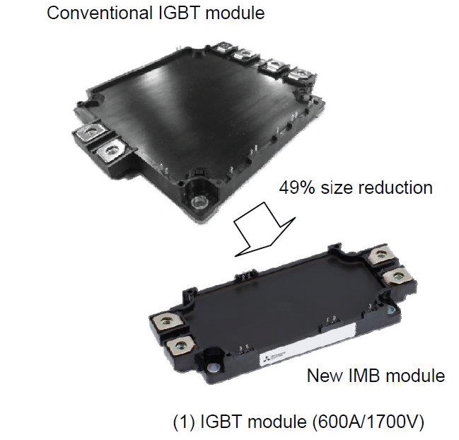
Figure 5: Example of the improved 1700V IGBT module by the new IMB
An example for the achievable package size reduction by improved IMB is shown in Figure 5. For the previous 6th generation 600A/1700V 2in1 module the package footprint was 122mm x 152mm; the 7th gen NX-type has a footprint of 62mm x 152mm, which corresponds to a 49% reduction.
Figure 6 shows a summary of the characteristics of the new and the conventional IMB. It is confi rmed by evaluation that the thermal resistance of the new IMB for the 1700V module is approximately 5% better than the conventional IMB for the 1200V module.
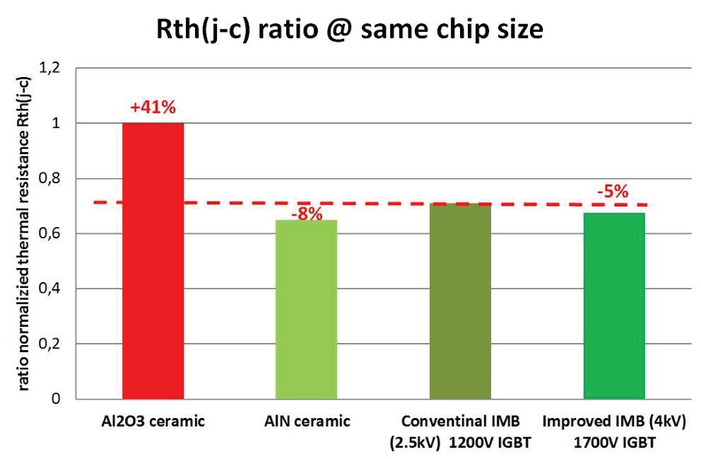
Figure 6: Comparison of thermal resistance Rth(j-c) ratio
On the other hand, the new IMB could also potentially reduce the thermal resistance for 650V and the 1200V class IGBT modules. Such combination of low loss 7th generation chips and the proposed improved SLC-Technology would enable us to increase the current density of the modules further. This option is currently under investigation.
High thermal cycling capability
The SLC-Technology utilizes layers with matched CTE-values as described above. Additionally the epoxy resin encapsulation can reduce the strain on the solder layer under the chip. [4] This ensures higher reliability during heat cycling and thermal cycling. Figure 7 shows the Scanning Acoustic Tomography (SAT) images by heat cycling test (-40~+125deg.C) at initial, 300 cycles and 600 cycles. Conventional structure had degradation of the solder layer under the ceramic substrate after 300 cycles. On the other hand, the new structure with the DP encapsulation has the solder layer only under the chip and no degradation after 600 cycles was observed. This result is the consequence of the elimination of the substrate solder layer and the utilization of the epoxy resin layer.
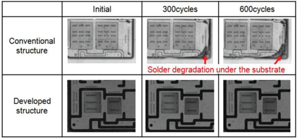
Figure 7: SAT images at diff erent number of cycles
Figure 8 shows the result of the thermal cycling test (ΔTc=80K (+45~+125°C)). The newly developed structure was tested until 40k cycles and has not failed yet. On the other hand, the conventional structure had degradation of the solder layer under the substrate (similar to the result of heat cycling). From this result, the new package with DP resin and IMB increases the thermal cycling life dramatically comparing with the conventional structure. This aspect is contributed by eliminating a solder layer under the insulator and thereby reducing the strain of solder layer under the chips.
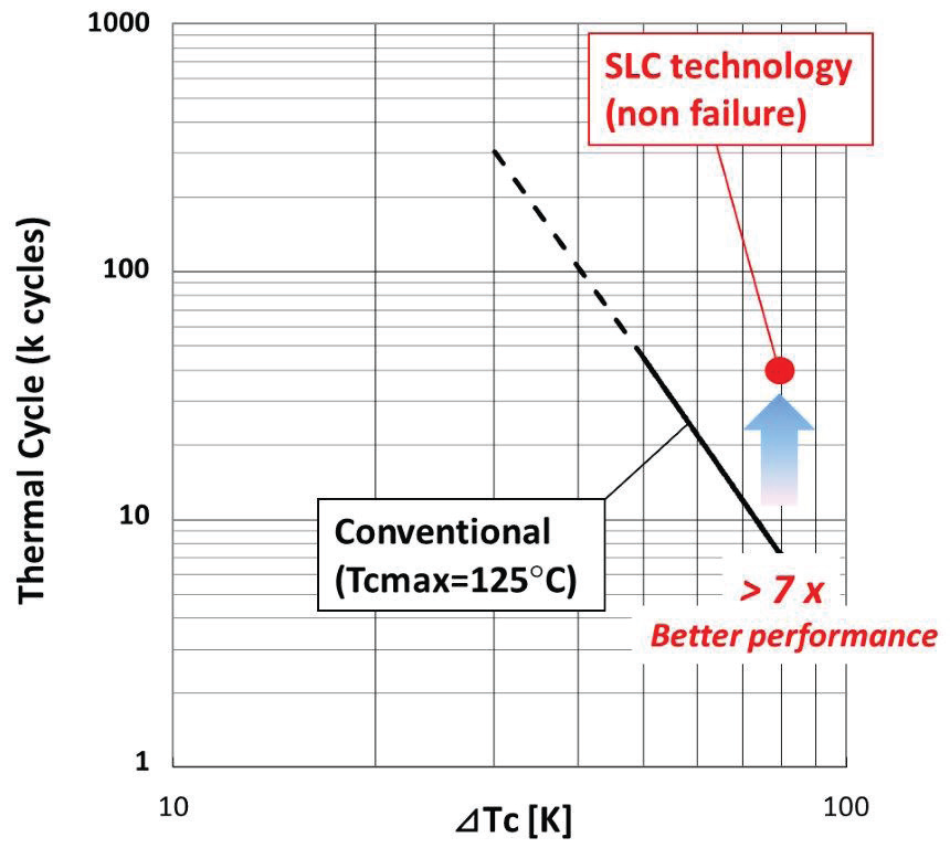
Figure 8: Thermal cycle test result of the SLC-Technology
SLC-Technology offers a ‘pumping-out-failure’ free package
The thermal resistance between the junction and the case has been successfully reduced by the improved IMB (as explained above). To achieve a higher power density and a high reliability, the thermal resistance Rth(c-s) between base plate and the heatsink must be optimized.
In general, thermal interface materials are applied between the base plate of the module and the cooling fin to get an enhanced thermal contact, and its parameters (such as thickness, performance, material property) have an impact on the heat dissipation capability and reliability [5]. On the other hand, it is well known that the shape of the base plate of the power module is deformed by temperature changes generated by power losses in the IGBT- and Diodes-chips. This small but repetitive deformation of the base plate pushes out the thermal interface material, and is referred-to as the “pumping out phenomenon”. For assuring a long-term stability in the thermal interface material, it is required to develop an advanced package structure which is capable of preventing the warpage of the base plate under continuous temperature cycles.
The conventional structure of the power module is shown in Figure 2 and their components along with their coefficients of thermal expansion (CTE) are described in Table. 1. In this structure, ceramic, solder and copper base plate, which are the constituents of module base, have different CTE-values. When the case temperature changes with the heat generated by the various IGBTs / FWDs operation, each component expands and contracts to different extents due to the different CTE-values. Finally, among the various layers, the differential strain results in differential deformation, such as with typical bimetal structures. This phenomenon is the cause of the base plate warpage.
The repetitive temperature change in a power module creates a repetitive warpage of the base plate as shown in Figure 9 (a) and (b). This warpage pushes out the thermal interface material. This pumping out phenomenon results in an ineffective thermal contact between the base plate and heatsink. This causes the degradation of Rth(c-s) and the heat dissipation capability of the power module. The consequence is an accelerated aging of the power module which in the worst case - results in the thermal destruction of the module when the junction temperature exceeds the absolute maximum rating.
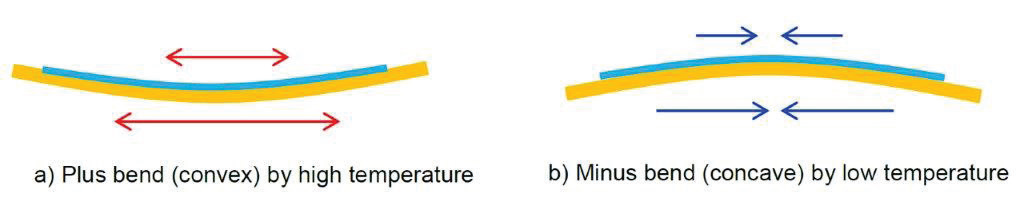
Figure 9: Phenomenon of baseplate warpage
The new package structure can dramatically reduce the differential strain between component materials of the module by matching their CTE-values. The internal structure of the package and their CTEvalues are described in Table 1 and Figure 2. This well-balanced (with respect to the CTE-values) structure results in much less deformation of the base plate caused by temperature change in comparison with a conventional structure. Figure 10 shows the result of the stress analysis (finite element method) for the base plate components (conventional and new structure respectively). The magnitude of the displacements shown in the Figure 10 have been enlarged by the same factor in order to make the differences more visible.
The simulation results depict that the new structure with the resin material has an improved response with respect to the base plate deformation during temperature changes.
For experimental verification, the vertical displacement of the baseplate center point was measured at three different ambient temperatures controlled by an environmental chamber. The reference length was 91mm in the longitudinal direction. The displacement measured during the temperature change from 25°C to 125°C resulted in only 13.4μm, which means that there was no significant warpage of the base plate. In the actual evaluation with a typical thermal interface material, no pumping out was found after 300 heat cycles (-40°C ~ +125 °C).
It is confirmed that the new power module structure, which has a matched coefficient of thermal expansion between adjacent layers, is able to minimize the warpage of base plate during temperature cycling and thereby provide a substantial reduction of the possibility of a pumping out failure event.
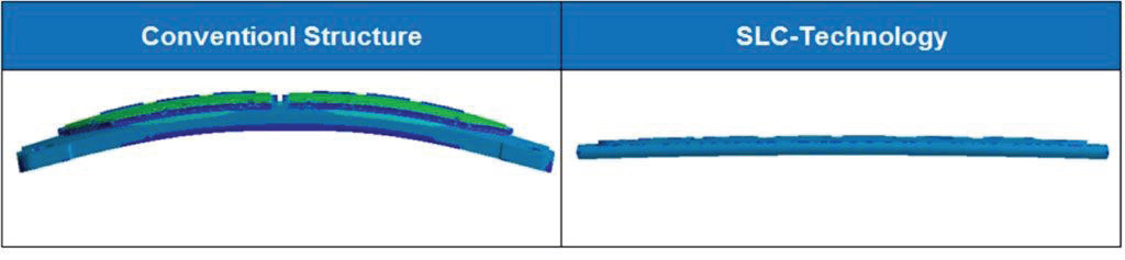
Figure 10: Finite element simulation results of baseplate warpage
Summary
The improved SLC-technology enables an expansion in the line-up of the 7th gen. NX-series IGBT modules to the 1700V class by utilizing the higher insulation voltage and the superior thermal conductivity of the improved IMB. This technology enables the development of a 600A/1700V module with a 122x62mm² footprint.
This SLC-Technology also offers a drastically improved thermal cycling capability in combination with the elimination of the pumpingout failures. The 7th gen chips provide excellent efficiency by the reduction of power losses. By combining this chip set with the SLCtechnology, the newly developed 7th gen NX-series IGBT provides an excellent answer to the requirements of power electronics systems such as high efficiency, high power density and high reliability.
References
[1] T. Radke et.al. “7th gen. IGBT and Diode chipset enabling highest performance power modules”, Bodo’s Power Systems, June 2015, p.30-32
[2] T. Radke et al., “More Power and Higher Reliability by 7th Gen. IGBT Module with New SLC-Technology”, Bodo’s Power Systems, August 2015, p.30-32
[3] T. Takahashi, et al: “A 1700V-IGBT module and IPM with new insulated metal baseplate (IMB) featuring enhanced isolation properties and thermal conductivity”, PCIM Europe 2016
[4] S. Asada, et al: “Resin Encapsulation Combined with Insulated Metal Baseplate for Improving Power Module Reliability”, PCIM Europe 2016,
[5] J. Yamada, et al:”Pumping out failure free package structure”, PCIM Europe 2016,
Articles similaires
Now available – DC/DC converters from PREMIUM
We introduced a novelty to our permanent offer in DACPOL in the category of power supplies and converters and today...
Read more
New release in DACPOL lighting for lathes – Kira covers
We introduce a new product into the DACPOL category of industrial lighting and today we offer KIRA covers for...
Read more
Laissez un commentaire