shopping_cart
Krepšelis
0,00 PLN
0
Iškarpinė
Jūs turite būti prisijungę
-
-
-
Category
-
Puslaidininkiai
- Diodai
- Tiristoriai
-
Elektroizoliuoti moduliai
- Elektrai izoliuoti moduliai | VISHAY (IR)
- Elektrai izoliuoti moduliai | INFINEON (EUPEC)
- Elektrai izoliuoti moduliai | Semikronas
- Elektrai izoliuoti moduliai | POWEREX
- Elektrai izoliuoti moduliai | IXYS
- Elektrai izoliuoti moduliai | POSEICO
- Elektrai izoliuoti moduliai | ABB
- Elektrai izoliuoti moduliai | TECHSEM
- Eikite į subkategoriją
- Lygintuviniai tilteliai
-
Tranzistoriai
- Tranzistoriai | GeneSiC
- SiC MOSFET moduliai | Mitsubishi
- SiC MOSFET moduliai | STARPOWER
- „ABB SiC MOSFET“ moduliai
- IGBT moduliai | MITSUBISHI
- Tranzistorių moduliai | MITSUBISHI
- MOSFET moduliai | MITSUBISHI
- Tranzistorių moduliai | ABB
- IGBT moduliai POWEREX
- IGBT moduliai INFINEON (EUPEC)
- Silicio karbido puslaidininkiniai elementai
- Eikite į subkategoriją
- Valdikliai
- Galios blokai
- Eikite į subkategoriją
- Elektrinių dydžių keitikliai
-
Pasyvūs komponentai (kondensatoriai, rezistoriai, saugikliai, filtrai)
- Rezistoriai
-
Saugikliai
- ABC ir AGC serijos miniatiūriniai saugikliai elektronikai
- Greitaeigiai cilindriniai saugikliai
- Uždelsimo elementai su GL/GG ir AM charakteristikomis
- Ultragreiti intarpai - saugikliai
- Didžiosios Britanijos ir JAV standartų greitaeigiai saugikliai
- Europos standarto greitaeigiai saugikliai
- Saugikliai geležinkeliui
- Aukštos įtampos saugikliai
- Eikite į subkategoriją
-
Kondensatoriai
- Kondensatoriai varikliams
- Elektrolitiniai kondensatoriai
- Snubbers tipo kondensatoriai
- Galios kondensatoriai
- Kondensatoriai DC grandinėms
- Kondensatoriai galios kompensavimui
- Aukštos įtampos kondensatoriai
- Kondensatoriai indukciniam kaitinimui
- Impulsiniai ir energijos kaupimo kondensatoriai
- DC LINK kondensatoriai
- AC / DC grandinių kondensatoriai
- Eikite į subkategoriją
- Slopinimo tinklo filtrai
- Superkondensatoriai
- Apsauga nuo viršįtampių
- Eikite į subkategoriją
-
Relės ir kontaktoriai
- Relių ir kontaktorių teorija
- Trijų fazių puslaidininkinės AC relės
- Puslaidininkinės DC relės
- Reguliatoriai, valdikliai ir jų priedai
- Soft starteriai (minkšto paleidimo įrenginiai) bei reversiniai kontaktoriai
- Elektromechaninės relės
- Kontaktoriai
- Rotaciniai jungikliai
-
Vienos fazės puslaidininkinės AC relės
- AC vienfazės puslaidininkinės relės 1 | D2425 | D2450 serijų
- AC vienfazės puslaidininkinės relės CWA ir CWD serijų
- AC vienfazės puslaidininkinės relės CMRA ir CMRD serijų
- AC vienfazės puslaidininkinės relės PS serijos
- AC puslaidininkinės dvigubos ir keturgubos relės D24 D, TD24 Q, H12D48 D serijų
- Vienfazės puslaidininkinės relės gn serijos
- AC vienfazės puslaidininkinės relės CKR serijos
- AC vienfazės relės DIN bėgiams ERDA ir ERAA serijų
- Vienfazės kintamosios srovės relės, skirtos 150A srovei
- Dvigubos kietojo kūno relės, integruotos su radiatoriumi DIN bėgiui
- Eikite į subkategoriją
- Vienos fazės puslaidininkinės AC relės spausdinimo plokštėms
- Interfejsų relės
- Eikite į subkategoriją
- Indukciniai elementai
- Radiatoriai, varistoriai, termo apsauga
- Ventiliatoriai
- Kondicioneriai, elektros spintų aksesuarai, aušintuvai
-
Baterijos, įkrovikliai, buferiniai maitinimo šaltiniai ir keitikliai
- Baterijos, įkrovikliai - teorinis aprašymas
- Ličio jonų baterijos. Individualios baterijos. Baterijų valdymo sistema (BMS)
-
Akumuliatoriai
- Panasonic įmonės akumuliatoriai
- SSB įmonės akumuliatoriai
- Sonnenschein Dryfit įmonės akumuliatoriai
- MK Battery įmonės geliniai akumuliatoriai
- FIAMM įmonės akumuliatoriai
- Victron Energy akumuliatoriai
- „Victron Energy LiFePO4“ akumuliatoriai
- „Dyno“ baterijos
- APC UPS RBC akumuliatorių paketai
- Eikite į subkategoriją
- Akumuliatorių įkrovikliai ir priedai
- UPS atsarginis maitinimo šaltinis ir buferiniai maitinimo šaltiniai
- Fotoelektros keitikliai ir priedai
- Energijos kaupimas
- Kuro elementai
- Ląstelės litio-joninės
- Eikite į subkategoriją
-
Automatikos komponentai
- Futaba Drone Parts
- Galiniai jungikliai, mikrojungikliai
- Jutikliai, keitikliai
- Pirometrai
- Skaitikliai, laiko relės, paneliniai matuokliai
- Pramoniniai apsaugos įrenginiai
- Šviesos ir garso signalizacija
- Terminio vaizdo kamera
- LED švieslentės
- Valdymo aparatūra - mygtukai ir jungikliai
-
Registravimo prietaisai
- AL3000 - įrašantis į juostą temperatūros registratorius su skaitmeniniu ekranu
- Mikroprocesoriniai registratoriai su LCD ekranu KR2000 serijos
- Registratorius KR5000
- Matuoklis su drėgmės ir temperatūros įrašymo funkcija HN-CH
- Registratorių reikmenys
- Grafinis kompaktinis registratorius 71VR1
- Registratorius KR 3000
- PC registratoriai R1M serijos
- PC registratoriai R2M serijos
- PC registratorius, 12 izoliuotų įėjimų – RZMS
- PC registratorius, USB, 12 izoliuotų įėjimų – RZUS
- Eikite į subkategoriją
- Eikite į subkategoriją
-
Laidai, pynės, laidų apsauginės žarnos, lankstūs sujungimai
- Laidai
- Daugiagisliai laidai
-
Kabeliai ekstremalioms sąlygoms
- Kompensaciniai ir prailginimo kabeliai
- Laidai termoporoms
- PT jutikliams prijungimo laidai
- Daugiagysliai laidai temp. -60C iki +1400C
- Vidutinės įtampos kabeliai
- Uždegimo laidai
- Šildymo laidai
- Viengysliai laidai temp. -60C iki +450C
- Geležinkelio kabeliai
- Šildymo kabeliai Ex zonoms
- Eikite į subkategoriją
- Apsaugos vamzdeliai
-
Pintinės
- Plokščios pintinės
- Apvalios pintinės
- Plokščios labai elastingos pintinės
- Apvalios labai elastingos pintinės
- Cilindro formos vario pintinės
- Vario cilindrinės pintinės su apsauga
- Elastingos įžeminimo juostos
- Cinkuoto ir nerūdijančio plieno cilindrinės pintinės
- PCV izoliuotos vario pintinės - temperatūra iki 85 C
- Plokščios aliuminio pintinės
- Sujungimo komplektas - pintinės ir vamzdeliai
- Eikite į subkategoriją
- Aksesuarai geležinkeliams
- Kabelių antgaliai
- Lanksčios izoliuotos šynos
- Daugiasluoksnės lanksčios šynos
- Laidų pravedimo sistemos (PESZLE)
- Gofruotos apsauginės žarnos
- Eikite į subkategoriją
- Žiūrėti visas kategorijas
-
Puslaidininkiai
-
-
New Horizons in Thermal Cycling Capability Realized with the 7th gen. IGBT Module Based on SLC-Technology

New Horizons in Thermal Cycling Capability Realized with the 7th gen. IGBT Module Based on SLC-Technology
In various power electronic applications, the lifetime of the converter is a key factor for consideration for estimating the total cost. Particularly at intermittent load profiles the lifetime of a power converter is limited by the temperature cycling capability of the power module packages due to the interconnection of materials with different CTEs (Coefficient of Thermal Expansion). The 7th gen. IGBT modules are based on the new SLC packaging technology with a material composition based on matching CTEs which result in the highest thermal cycling capability.
By Thomas Radke, Narender Lakshmanan, Mitsubishi Electric Europe B.V
Introduction
The 7th gen. NX-type IGBT modules in the 650V, the 1200V and the 1700V categories have been developed in a comprehensive line-up to provide the best solution for different power classes. The new CIB (Converter Inverter Brake) modules which have been recently developed and the 800A / 1200V half bride module will further extend the line-up. The 7th gen. NX-type IGBT modules and the G1-series IPMs are based on the SLC package technology offering a remarkable advancement in the level of the thermal cycling capability. This improved thermal cycling capability can be exploited to extend the inverter lifetime. A lifetime extension essentially reduces the total cost, because the system can operate longer and new investments can be postponed.
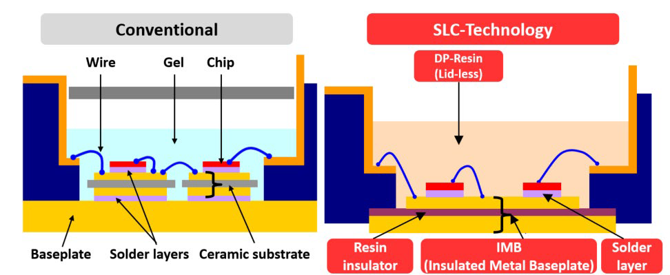
Figure 1: Comparison of SLC and conventional package structures
SLC-Technology
SLC (SoLid Cover) -Technology is a newly developed package technology for realizing power semiconductor modules with high reliability and high thermal conductivity [3]. The comparison of the SLC package structure with a conventional module structure is shown in Figure 1. As it can be noticed from Figure 1, the SLC-Technology possess a significantly altered package design in comparison to the conventional module structure.
The soft silicone gel of the conventional structure is replaced by the hard DP-resin (direct potting resin). This hard encapsulation with DP-resin, which has an optimized CTE (Coefficient of Thermal Expansion), prevents the degradation of the chip solder [3].
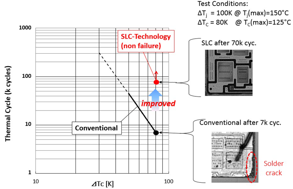
Figure 2: Thermal cycle test status
The conventionally used ceramic insulation layer is replaced by a resin insulation material in the SLC-Technology. This resin insulation material has a CTE value matching with that of copper. Both copper as well the resin insulator have a CTE of about 17ppm/K as shown in Table 1. Therefore, in case of temperature cycling, there is no mechanical stress caused by the mismatch in the CTE values between the copper baseplate and the insulation layer. Furthermore, the baseplate solder layer is completely eliminated because the top and bottom side copper layers are directly bonded to the insulating resin layer. Employing this IMB (Insulated Metal Baseplate) in combination with the hard encapsulation (DP-resin), the thermal cycling capability is substantially improved. The status of the ongoing thermal cycle test is presented in Figure 2. Currently, a level of 70k cycles has been already achieved. The test was conducted for a temperature swing of ΔTc=80K at the case and ΔTj=100K at the IGBT junction. This result is about 10 times higher than the conventional capability, and this test is still ongoing since the module’s failure point has not yet been encountered. Furthermore, as shown on the right side of Figure 2, even after 70k cycles no delamination at all could be observed and therefore, an even higher thermal cycling capability is expected.
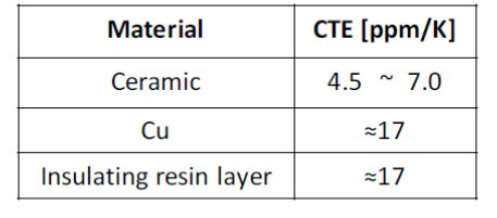
Table 1: Table with Coefficient of Thermal Expansion
In the conventional module packaging structure, the metallized ceramic substrates are utilized to realize the electrical insulation between the electrical circuit (consisting of the semiconductor chips) and the module’s base plate. The substrate layer is fixed to the copper base plate by a solder layer. The drawback of this arrangement is evident from the nature of the resulting material combination - the mismatch of CTE between ceramic, solder and copper. Depending on the ceramic material employed, the insulator CTE is in range of 4.5~7 ppm/K as shown in Table 1. This mismatch causes solder cracks during temperature swings and limits the lifetime of the power modules. As shown in Figure 2, after 7k cycles (with a swing of ΔTc=80K), the solder layer begins to crack.
Load Cycles in Power Applications
Load cycles have to be considered in almost all power electronic applications. The load profile depends on the individual application
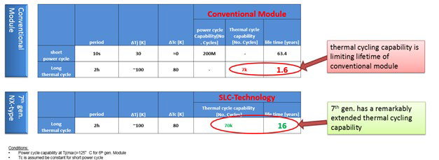
Figure 3: Application example for load cycling
conditions. In applications such as machine tools or servo drives, the occurrence of a high number of load cycles within a relatively short duration has to be considered. Load cycles typically occur in the form of short pulses possessing a time duration in the range of a few seconds. Since the thermal time constant of the heatsink is in the range of a few minutes, it can be assumed that the heatsink temperature remains constant between successive load cycle pulses. The number of maximum allowable junction temperature swing (ΔTj) for applications requiring significant load cycling for its normal operation, is usually limited by the inverter design (for eg –limited to about 30K) to offer an acceptable power cycle lifetime. Also, higher temperature swings and thermal cycles have to be considered in case the system temporarily pauses operation based on a discontinuous operating sessions wherein the entire heatsink may cool down to the ambient temperature. For air-cooled heat sinks, this cooling down takes a couple of minutes due to the nature of the heatsink thermal time constant. For a liquid cooled inverter, the cooling down process is faster since just some tens of seconds are sufficient to cool down the total system. That means if an inverter is used in a production process which is discontinuous, either due to tuning/adjustment requirements, breaks taken by the machine operator or due to interrupted flow of materials - thermal cycling also has to be taken into consideration. Similar considerations have to be taken also for certain other application like cranes or elevators where the power converters do not operate continuously. If we consider typical operational IGBT junction temperature of 125°C and an ambient temperature of 25°C, the junction temperature swing(ΔTj) will be in the range of 100K in case of such intermittent inverter operation. The temperature cycling capability has approximately an inverse exponential dependency with the temperature swing. Therefore, considering the power cycling capability curve of a conventional IGBT module, the ΔTj=100K swing causes dramatically higher relative aging compared to the ΔTj=30K swing. Due to that fact that the total system pauses the operation for several minutes, we can assume that also the IGBT case temperature will also experience a temperature swing of about ΔTc=80K.
In figure 3, an example of an application is provided. If we consider a process where one load cycle occurs every 10 seconds, and the temperature rise of about 30K the power cycle capability for ΔTj=30K is about 200 million cycles which means the inverter lifetime can be estimated to reach a total operational lifetime of about 63 years which is acceptable. But if we have to consider an interrupted process chain and assume that the inverter operation is interrupted every 2 hours for a couple of minutes, the thermal cycling capability of the power module has to be taken into consideration. For a case temperature swing of about 80K (ΔTc=80K) the thermal cycling capability of a conventional module is limited to about 7000 cycles which, under the assumed operation conditions, would be equivalent to about 1.6 years of total operational lifetime. Considering that the 7th gen with the SLC technology has a thermal cycling test result of more than 70k cycles we can expect a remarkable extension of operational lifetime, in this example, will be extended to more than 16 year of operation. In conclusion, it can be stated that for various applications where non continuous operation has to be considered, the lifetime of power converters can be significantly improved by utilization the of 7th gen. NX-type IGBT Module based on SLC-Technology.
Line-up Expansion
As a first step, the 7th gen. NX-Type IGBT modules are developed in the blocking voltage classes : 650V and 1200V. The 6in1 and 7in1 topology modules are developed covering current ratings from 100A to 200A. The 2in1 modules in the M-size (62x152mm²) package cover the current ratings from 225A~600A. To realize a further expansion of the current ratings toward higher blocking voltages and higher rated currents, an improved resin insulation layer material - the IMB-technology was developed. The new resin material provides a higher thermal conductivity while simultaneously maintaining the high electrical insulation capability [2]. The utilization of this improved material enables a reduction in the thermal impedance that enables the development of modules with higher rated currents. This technology has now been applied and an 800A/1200V 2in1 module is under development in the M-size package. On the other hand, the improved thermal conductivity enables an increase in the insulation layer thickness without a negative impact on the resulting thermal resistance. By this approach, an insulation capability of 4kV has been achieved and this is utilized to realize to modules with a blocking voltage of 1700V [4].
In addition to the expansion towards higher current levels and higher voltage levels, the development of modules with CIB-topology for the current ratings between 35A and 150A has been initiated. These CIB configuration modules consist of a three-phase input rectifier bridge, a brake chopper and a three-phase output inverter. For the smaller current ratings, a 45x107.5mm S-size package is under development. To be compatible to the de-facto standards as much as possible, the IGBT housing for this CIB module is now available in the market with two different pin terminal configurations. Furthermore, all CIB modules will be made available in the market with both the solder pin terminal version and the press-fit pin terminal version.
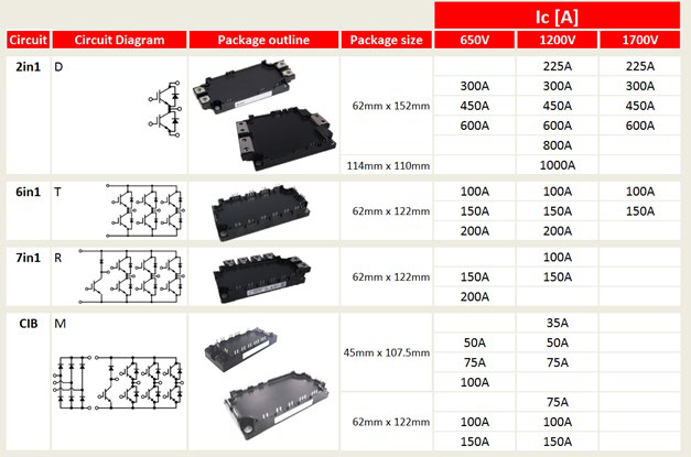
Figure 4: Line-up of 7th gen NX-type IGBT modules
New 1700V Modules - Optimized for High Efficiencies
IGBT modules with 1700V blocking capability are mainly used for inverters with 690Vac output voltage. The applied dc-link voltage “VCC” is in the range of 1000V~1200V and essentially higher than that required by inverters intended to deliver 400Vac (which require 1200V category IGBT modules). The higher applied voltage results in higher switching losses due to the higher voltage at the transition of collector emitter voltage. This is the reason why inverters utilizing the 1700V IGBT modules are usually operated at lower switching frequencies compared to an inverter using the 1200V IGBT modules. As a result, in conventional 1700V IGBT modules, the switching losses become the dominant part even at low switching frequencies. Therefore, the switching losses have been identified as the bottleneck for the IGBT module performance in industrial inverter mode applications. For the chip design of the 1700V, the 7th gen IGBT and the diode chipset, this has been considered and counter measures have been taken. In Figure 5 the Eoff vs VCEsat tradeoff is shown and it represents the IGBT chip performance. During the chip design, the IGBT characteristics can be tuned to achieve lower conduction losses or lower switching losses. If, for example - an IGBT chip design is optimized for very low VCEsat , the switching losses tend to be high and vice versa - an IGBT chip design which is optimized for low switching losses tend to have a high VCEsat. As shown in Figure 5, the 7th gen 1700V device offers both lower switching and lower conduction losses. This means that the overall chip performance is improved and is better than the conventional chip. The conduction losses are slightly better but the switching losses are essentially improved by about 40%. Apart from the IGBT chip, the 7th gen. 1700V diode which based on the RFC structure (relaxed field of cathode) has an improved overall performance and is tuned for operations at high switching frequencies. In Figure 6, the loss comparison (which was prepared by using the Melcosim software [1]) of a 600A/1200V module (CM600DX-34T) versus a conventional 600A/1700V IGBT module under a typical inverter mode operation condition is shown. The improved chip characteristics result in a loss reduction of 7.4% at a switching frequency of 0.5 kHz. For higher carrier frequencies, the improvement becomes more significant. Therefore, with 1 kHz the loss reduction is 16.4%, with 2.0 kHz the reduction is 25.8%, and with 4 kHz 33.6% of the losses can be saved. This loss saving will improve the power converter efficiency, and in-turn contribute to the energy savings and eco-friendly operation. Apart from the energy, enabling loss reduction will lead to lower operation temperatures and therefore facilitate increasing the load of the inverter. Therefore by utilizing this new 7th gen. 1700V chipset enables designing the inverter with higher power density and cost optimization.
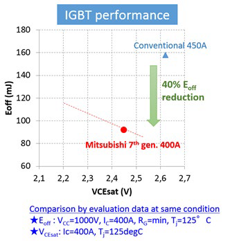
Figure 5: Eoff vs. VCEsat trade-off comparison of 7th gen. 1700V IGBT chip
Summary
The 7th gen NX-type IGBT module offers an enormously improved life time by utilization of the SLC-Technology. Matching and optimizing the CTEs of the SLC package Technology opens-up this new horizon in thermal cycling capability. An example application has demonstrated that a significantly higher lifetime can be achieved. This technology is now available in a comprehensive line-up, which has been expanded to include CIB modules and the 1700V category modules. The new 1700V IGBTs and the diode chip sets have a trade-off optimization of the switching characteristics and the conduction characteristics which result in a significantly higher efficiency and overall module performance.
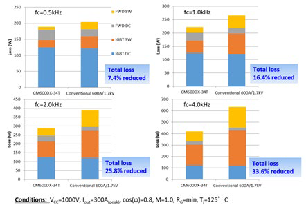
Figure 6: Loss comparison of 1700V IGBT modules
References
[1] MELCOSIM: IGBT thermal and loss simulation software, available at www.mitsubishielectric.com/semiconductors/ simulator/
[2] T. Takahashi, et al: “A 1700V-IGBT module and IPM with new insulated metal baseplate (IMB) featuring enhanced isolation properties and thermal conductivity”, PCIM Europe 2016, page 342-347
[3] S. Asada, et al: “Resin Encapsulation Combined with Insulated Metal Baseplate for Improving Power Module Reliability”, PCIM Europe 2016, page 326-330
[4] Thomas Radke, et al: Enhanced IGBT Module Power Density Utilizing the Improved Thermal Conductivity of SLC-Technology, Bodo’s Power systems, June 2016
Related posts
Now available – DC/DC converters from PREMIUM
We introduced a novelty to our permanent offer in DACPOL in the category of power supplies and converters and today...
Read more
New release in DACPOL lighting for lathes – Kira covers
We introduce a new product into the DACPOL category of industrial lighting and today we offer KIRA covers for...
Read more
Leave a comment