shopping_cart
Krepšelis
0,00 PLN
0
Iškarpinė
Jūs turite būti prisijungę
-
-
-
Category
-
Puslaidininkiai
- Diodai
- Tiristoriai
-
Elektroizoliuoti moduliai
- Elektrai izoliuoti moduliai | VISHAY (IR)
- Elektrai izoliuoti moduliai | INFINEON (EUPEC)
- Elektrai izoliuoti moduliai | Semikronas
- Elektrai izoliuoti moduliai | POWEREX
- Elektrai izoliuoti moduliai | IXYS
- Elektrai izoliuoti moduliai | POSEICO
- Elektrai izoliuoti moduliai | ABB
- Elektrai izoliuoti moduliai | TECHSEM
- Eikite į subkategoriją
- Lygintuviniai tilteliai
-
Tranzistoriai
- Tranzistoriai | GeneSiC
- SiC MOSFET moduliai | Mitsubishi
- SiC MOSFET moduliai | STARPOWER
- „ABB SiC MOSFET“ moduliai
- IGBT moduliai | MITSUBISHI
- Tranzistorių moduliai | MITSUBISHI
- MOSFET moduliai | MITSUBISHI
- Tranzistorių moduliai | ABB
- IGBT moduliai POWEREX
- IGBT moduliai INFINEON (EUPEC)
- Silicio karbido puslaidininkiniai elementai
- Eikite į subkategoriją
- Valdikliai
- Galios blokai
- Eikite į subkategoriją
- Elektrinių dydžių keitikliai
-
Pasyvūs komponentai (kondensatoriai, rezistoriai, saugikliai, filtrai)
- Rezistoriai
-
Saugikliai
- ABC ir AGC serijos miniatiūriniai saugikliai elektronikai
- Greitaeigiai cilindriniai saugikliai
- Uždelsimo elementai su GL/GG ir AM charakteristikomis
- Ultragreiti intarpai - saugikliai
- Didžiosios Britanijos ir JAV standartų greitaeigiai saugikliai
- Europos standarto greitaeigiai saugikliai
- Saugikliai geležinkeliui
- Aukštos įtampos saugikliai
- Eikite į subkategoriją
-
Kondensatoriai
- Kondensatoriai varikliams
- Elektrolitiniai kondensatoriai
- Snubbers tipo kondensatoriai
- Galios kondensatoriai
- Kondensatoriai DC grandinėms
- Kondensatoriai galios kompensavimui
- Aukštos įtampos kondensatoriai
- Kondensatoriai indukciniam kaitinimui
- Impulsiniai ir energijos kaupimo kondensatoriai
- DC LINK kondensatoriai
- AC / DC grandinių kondensatoriai
- Eikite į subkategoriją
- Slopinimo tinklo filtrai
- Superkondensatoriai
- Apsauga nuo viršįtampių
- TEMPEST spindulių aptikimo filtrai
- Viršįtampių ribotuvas
- Eikite į subkategoriją
-
Relės ir kontaktoriai
- Relių ir kontaktorių teorija
- Trijų fazių puslaidininkinės AC relės
- Puslaidininkinės DC relės
- Reguliatoriai, valdikliai ir jų priedai
- Soft starteriai (minkšto paleidimo įrenginiai) bei reversiniai kontaktoriai
- Elektromechaninės relės
- Kontaktoriai
- Rotaciniai jungikliai
-
Vienos fazės puslaidininkinės AC relės
- AC vienfazės puslaidininkinės relės 1 | D2425 | D2450 serijų
- AC vienfazės puslaidininkinės relės CWA ir CWD serijų
- AC vienfazės puslaidininkinės relės CMRA ir CMRD serijų
- AC vienfazės puslaidininkinės relės PS serijos
- AC puslaidininkinės dvigubos ir keturgubos relės D24 D, TD24 Q, H12D48 D serijų
- Vienfazės puslaidininkinės relės gn serijos
- AC vienfazės puslaidininkinės relės CKR serijos
- AC vienfazės relės DIN bėgiams ERDA ir ERAA serijų
- Vienfazės kintamosios srovės relės, skirtos 150A srovei
- Dvigubos kietojo kūno relės, integruotos su radiatoriumi DIN bėgiui
- Eikite į subkategoriją
- Vienos fazės puslaidininkinės AC relės spausdinimo plokštėms
- Interfejsų relės
- Eikite į subkategoriją
- Indukciniai elementai
- Radiatoriai, varistoriai, termo apsauga
- Ventiliatoriai
- Kondicioneriai, elektros spintų aksesuarai, aušintuvai
-
Baterijos, įkrovikliai, buferiniai maitinimo šaltiniai ir keitikliai
- Baterijos, įkrovikliai - teorinis aprašymas
- Ličio jonų baterijos. Individualios baterijos. Baterijų valdymo sistema (BMS)
- Akumuliatoriai
- Akumuliatorių įkrovikliai ir priedai
- UPS atsarginis maitinimo šaltinis ir buferiniai maitinimo šaltiniai
- Fotoelektros keitikliai ir priedai
- Energijos kaupimas
- Kuro elementai
- Ląstelės litio-joninės
- Eikite į subkategoriją
-
Automatikos komponentai
- Spiralift keltuvai
- Futaba dronų dalys
- Galiniai jungikliai, mikrojungikliai
- Jutikliai, keitikliai
- Pirometrai
- Skaitikliai, laiko relės, paneliniai matuokliai
- Pramoniniai apsaugos įrenginiai
- Šviesos ir garso signalizacija
- Terminio vaizdo kamera
- LED švieslentės
- Valdymo aparatūra - mygtukai ir jungikliai
- Eikite į subkategoriją
-
Laidai, pynės, laidų apsauginės žarnos, lankstūs sujungimai
- Laidai
- Kabelių įvadai ir movos
- Daugiagisliai laidai
-
Kabeliai ekstremalioms sąlygoms
- Kompensaciniai ir prailginimo kabeliai
- Laidai termoporoms
- PT jutikliams prijungimo laidai
- Daugiagysliai laidai temp. -60C iki +1400C
- Vidutinės įtampos kabeliai
- Uždegimo laidai
- Šildymo laidai
- Viengysliai laidai temp. -60C iki +450C
- Geležinkelio kabeliai
- Šildymo kabeliai Ex zonoms
- Eikite į subkategoriją
- Apsaugos vamzdeliai
-
Pintinės
- Plokščios pintinės
- Apvalios pintinės
- Plokščios labai elastingos pintinės
- Apvalios labai elastingos pintinės
- Cilindro formos vario pintinės
- Vario cilindrinės pintinės su apsauga
- Elastingos įžeminimo juostos
- Cinkuoto ir nerūdijančio plieno cilindrinės pintinės
- PCV izoliuotos vario pintinės - temperatūra iki 85 C
- Plokščios aliuminio pintinės
- Sujungimo komplektas - pintinės ir vamzdeliai
- Eikite į subkategoriją
- Aksesuarai geležinkeliams
- Kabelių antgaliai
- Lanksčios izoliuotos šynos
- Daugiasluoksnės lanksčios šynos
- Laidų pravedimo sistemos (PESZLE)
- Eikite į subkategoriją
- Žiūrėti visas kategorijas
-
Puslaidininkiai
-
-
Line-up Expansion of X-Series High Voltage IGBT Modules in the 3300 V Class

Line-up Expansion of X-Series High Voltage IGBT Modules in the 3300 V Class
The 3300 V X-Series continues the success story of the R- and the H-Series power modules of Mitsubishi Electric by improving the overall performance of the device.
By Eugen Wiesner and Eugen Stumpf Mitsubishi Electric Europe B. V. and H. Uemura Mitsubishi Electric Corporation
Introduction
Major applications using 3300 V IGBT modules like traction, medium voltage drives or power transmission & distribution require an absolute minimization of the number of fi eld failures. Taking into consideration all possible worst case application conditions, it must be ensured that the device must be operated safely inside the technical specifi cation. But in reality, it is sometimes impossible to predict all the worst case conditions which might occur during an actual fi eld operation. That is the reason behind the requirement which states that IGBT modules must have reasonable margin between the parameters representing the module specifi cations and the critical operation of the module. The 3300 V X-Series was developed to improve the device durability, reliability and to further minimize the failure probability during an actual operation in the fi eld. This article describes the basic points of the X-Series design including the improvements contributing to a safe operation of the device to ensure an overall good performance.
Seventh Generation 3300 V IGBT chip
The fi rst 3300 V modules (H-Series) were released by Mitsubishi Electric in 1997. The IGBT chip performance has been continuously improved over time since the release of the fi rst generation. The fi rst H-Series power devices have a planer gate IGBT chip structure. The subsequent R-Series devices utilize an improved planar gate structure thereby allowing a wide operation temperature range from -50 °C to 150 °C. Furthermore a reduction of power losses and an increase in the module power density was achieved.
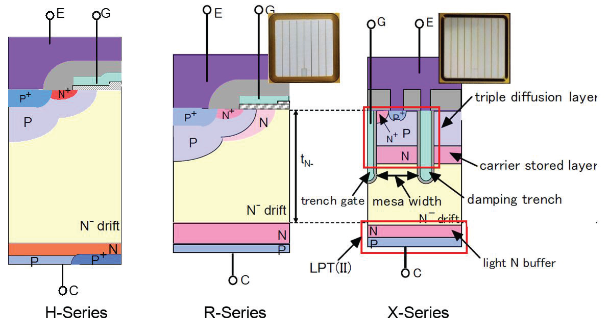
Figure 1: 3300V IGBT chip evolution
The development sequence of the 3300 V IGBT chips has been represented in Figure 1. The X-Series 3300 V IGBT chips contribute to a further increase in the module power density and an additional improvement in the IGBT power module characteristics. The CM1800HC-66X will be the fi rst device out of this new 3,3 kV X-Series that will be available in Q2/2017. It has the current rating of 1800A, it is a standard package with a foot print of 190 mm x 140 mm possessing an isolation voltage of 6 kV(AC).
Trade-off for Optimizing the IGBT Performance
The Figure 2 shows the fundamental triangular trade-off relationship of the IGBT power device. Three main parameters – the IGBT forward voltage (VCE(sat)), the turn off energy (EOFF) and the safe operating area (SOA) are strongly related to each other [1]. Additionally, the Short Circuit Safe Operating Area (SCSOA) is an important parameter which aff ects the optimization potential of other parameters. The consequent improvement of one parameter - like the reduction of the IGBT forward voltage may cause the increase of the short circuit current. The short circuit time tSC representing the SCSOA will thus be reduced.
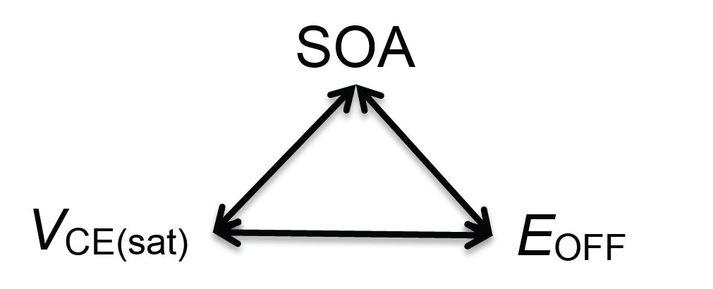
Figure 2: Fundamental trade-off for IGBT characteristics
The X-Series 3300 V IGBT chip was designed to provide an optimized and a balanced performance between IGBT forward voltage VCE(sat), turn-off switching energy EOFF and safe operating area. The design target was to maintain the 10 μs short circuit time (which is an existing market standard) along with a reasonable safety margin. The VCE(sat) versus EOFF trade-off curve of the X-Series is shown in Figure 3. The forward voltage was reduced by about 30% compared to the previous planar R-Series devices. The turn-off energy was maintained on the same level. This improvement was possible by adopting the trench gate structure CSTBT(III)TM and increasing the active chip area. The increase of the active chip area was possible by using an advanced guard-ring structure [2].
Even with such an improvement in the forward voltage, the short circuit current is relatively low thereby permitting the utilization of a short circuit time duration of 10 μs. To design a power module with adequate safety and reliability, it is also important to know the real limitation of the module. In this regard, the module will be tested to ascertain the point of failure and the device under test therefore will be subjected to extended short circuit time duration. Figure 4 shows the typical short circuit measurement result with CM1800HC-66X module at maximum operation conditions of TJ=150 °C and VCC=2500 V with a time duration of 15 μs. Apart from the short circuit energy, the short circuit time is also a parameter which indicates the short circuit device capability. With respect to the test result mentioned in Figure 4, the short circuit energy dissipated was more than 250 J. The 15μs time duration is 50% higher compared to the standard value of 10 μs, although the device could withstand 15 μs without failure.
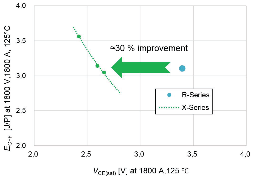
Figure 3: trade off VCE(sat) vs. EOFF at TJ=125°C
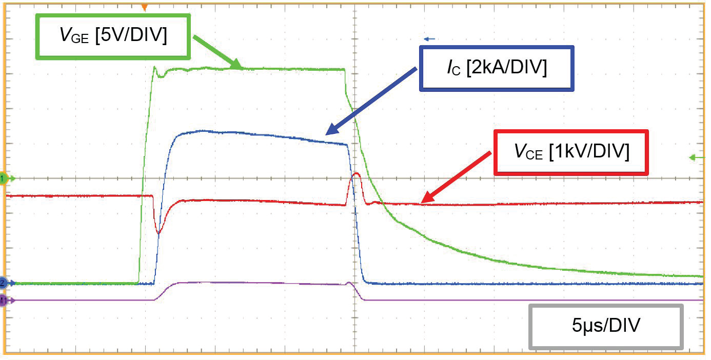
Figure 4: typical short circuit evaluation waveforms at TJ=150 °C, VCC=2500 V
The durability of the 7th Gen. IGBT chip to endure short circuit types II and III was already demonstrated with the X-Series fi rst runner 6500 V power module - CM1000HG-130XA [3].
Furthermore, the contribution of the guard-ring size reduction is the improvement of the thermal resistance between junction and case. Compared to the R-Series, the thermal resistance (junction to case) was improved by about 11% for the IGBT and by about 8% for the diode. This also contributes to enhancement of the module power density.
Case Study for Inverter Operation
The overall electrical and thermal performance characteristics improvement can be represented by simulation result in the three phase inverter operation. The diagram in Fig. 5 shows the simulation result of the normalized RMS output current versus switching frequency under the conditions: VCC=1800 V, m=1, cos(φ)=0,9, TJ=150 °C and the junction to case temperature increase of 10 K. At the switching frequency of 300 Hz, the RMS output current of CM1800HC-66X power module can be increase by about 20% compared to CM1500HC-66R device.
The CM1800HC-66X was designed not only to deliver good electrical performance, but also to withstand harsh environmental conditions like high humidity. The part of the module that is most sensitive to humidity is the chip guard ring area. With the newly adopted Surface Charge Control (SCC) technology, it is possible to control the surface charge in the guard ring area to achieve signifi cant humidity withstand capability even when the guard ring width is reduced [4].
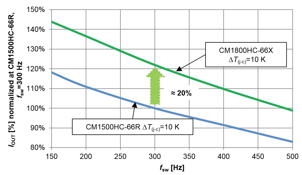
Figure 5: Inverter output current versus switching frequency at VCC=1800 V, cos(φ)=0,9, m=1, TJ=150 °C.
Conclusion
The new CM1800HC-66X power module allows an improvement in the converter design by reducing the power losses or increasing the converter power density. Furthermore it continues MITSUBISHI’s tradition of delivering high reliability and enabling a durable design in the 3300 V class IGBT power modules.
References
[1] T. Minato and H. Takahashi, “New Power-Element Technology”, Mitsubishi Electric ADVANCE, pp. 24-27, 2004.
[2] Ze Chen, et al, “A balanced High Voltage IGBT Design with Ultra Dynamic Ruggedness and Area-effi cient Edge Termination,” Proc. ISPSD 2013, p 37, Kanazawa, Japan.
[3] N. Tanaka, “Durable Design of the new HVIGBT Module”, PCIM 201 5.
[4] Sh. Honda, “High Voltage Device Edge Termination for Wide Temperature plus Humidity with Surface Charge Control Technology”, ISPSD 2016.
Related posts
Now available – DC/DC converters from PREMIUM
We introduced a novelty to our permanent offer in DACPOL in the category of power supplies and converters and today...
Read more
New release in DACPOL lighting for lathes – Kira covers
We introduce a new product into the DACPOL category of industrial lighting and today we offer KIRA covers for...
Read more
Leave a comment